
Lead Time Optimization: How to Reduce PCB Manufacturing Time
PCB manufacturing lead time directly impacts your product launch schedule and market competitiveness. In electronics development, a 2-week delay in prototypes can push your time-to-market by months when you account for multiple design iterations and validation cycles.
This guide explains the actual factors controlling PCB lead time, the specific design and procurement strategies that reduce manufacturing time, and the trade-offs between speed and cost. You will learn how to structure your project to hit aggressive schedules without compromising quality or inflating costs unnecessarily.
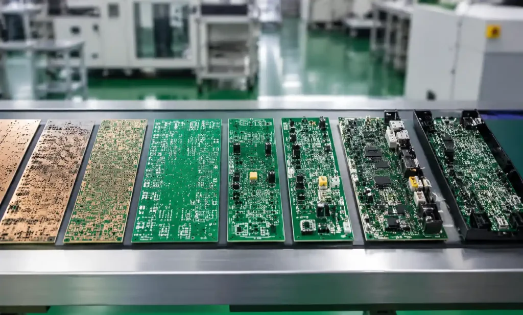
Understanding PCB Lead Time Components
PCB lead time is not a single number. It spans multiple sequential and parallel processes, each with its own duration. The total timeline depends on board complexity, material availability, production queue, and your data package quality.
A typical standard lead time breaks down into these stages: engineering review and DFM analysis (1-2 days), material procurement (2-5 days), fabrication processes including imaging, etching, drilling, and plating (3-7 days), surface finish application (1-2 days), electrical testing and inspection (1 day), and final packaging plus shipping (1-3 days). For a standard 4-6 layer FR-4 board, this totals 10-20 days. Quick turn services can compress this to 3-7 days by running steps in parallel and prioritizing your order.
| Lead Time Stage | Standard Duration | Quick Turn Duration | Key Variables |
|---|---|---|---|
| Engineering review + DFM | 1-2 days | 4-8 hours | File completeness, design complexity |
| Material procurement | 2-5 days | Same-day (stock items) | Material type, inventory levels |
| Fabrication (etch, drill, plate) | 3-7 days | 1-3 days | Layer count, via types, panel utilization |
| Surface finish | 1-2 days | 4-8 hours | Finish type (HASL, ENIG, OSP) |
| Testing + inspection | 1 day | 4-8 hours | Test requirements, pass rate |
| Packaging + shipping | 1-3 days | Express options | Destination, customs |
The stages that compress most easily are fabrication and finishing, because manufacturers can dedicate equipment and run smaller batches. The stages that resist compression are material procurement and any rework loops triggered by design issues.
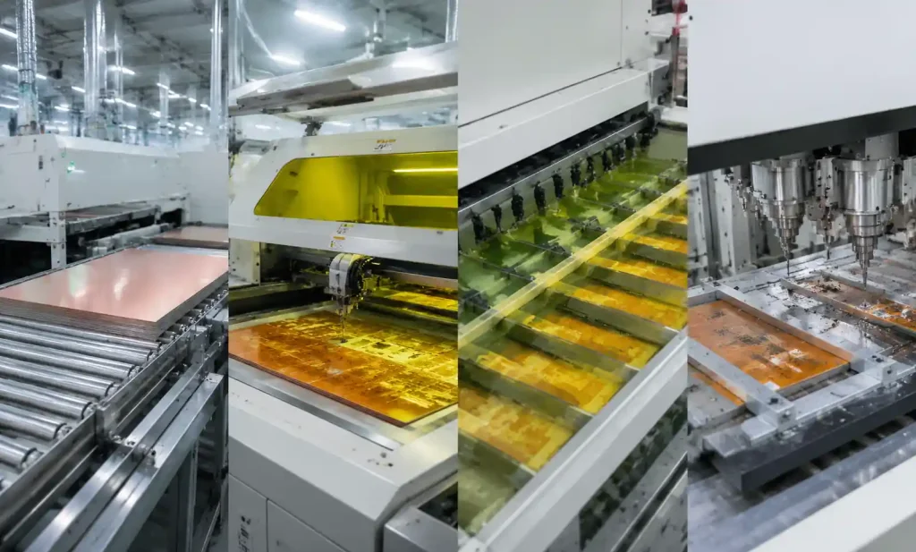
Design Factors That Control Manufacturing Speed
Your design choices set the ceiling on how fast any manufacturer can build your board. Complex specifications force sequential processing that cannot be accelerated, while standard configurations allow parallel workflows and quick turns.
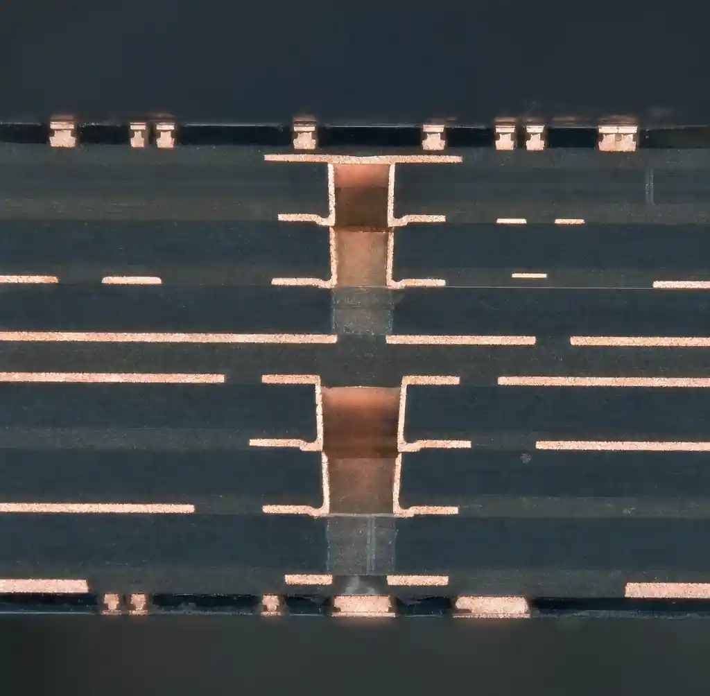
Layer count and stackup complexity: A 2-4 layer board with standard FR-4 material fabricates in 1-3 days, while an 8-10 layer HDI board with multiple lamination cycles requires 5-10 days minimum. Each additional lamination cycle adds 1-2 days because the board must cool, stabilize, and pass inspection before the next layer bonds. For fastest turnaround, specify 4-6 layers with symmetric stackup and avoid blind and buried vias unless density demands them.
Via technology and hole sizes: Through-hole vias drill mechanically in one pass, allowing same-day drilling for hundreds of boards. Laser-drilled microvias in HDI PCBs require sequential processing, adding 2-3 days per via layer. Standard 0.3mm finished hole size drills faster than 0.15mm microvias because larger bits tolerate higher spindle speeds and require fewer passes.
Material selection and availability: Standard FR-4 with Tg 130-140°C ships from stock at most manufacturers, enabling same-day material release. High-frequency materials like Rogers RO4003C or polyimide flex cores often require 5-15 day procurement unless you confirm stock before ordering. For controlled impedance boards, specify common dielectric constants (4.2-4.6 for FR-4) rather than exotic values that require custom material orders.
Surface finish choice: HASL (Hot Air Solder Leveling) applies in 2-4 hours because it is a single-pass convection process. ENIG (Electroless Nickel Immersion Gold) requires 8-12 hours for the nickel plating bath and gold immersion, plus stabilization time. OSP (Organic Solderability Preservative) finishes fastest at 1-2 hours but offers shorter shelf life. Choose HASL or OSP for prototypes where speed matters more than flatness.
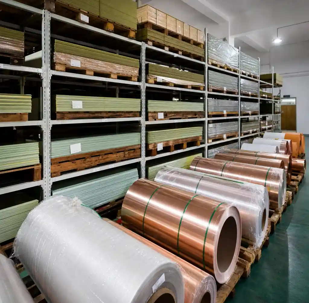
Material Procurement and Inventory Strategy
Material availability determines whether your board starts production today or waits 2 weeks. Manufacturers maintain stock for high-volume materials but special-order everything else, and those orders sit outside the quoted lead time.
Standard FR-4 laminate in common thicknesses (0.4mm, 0.8mm, 1.6mm) with standard copper weights (1oz, 2oz) ships from distributor stock within 1 day. The moment you specify non-standard thickness (0.6mm, 2.0mm), high-Tg material (Tg 170°C+), heavy copper (4oz, 6oz), or Rogers laminates, procurement extends to 5-20 days depending on supplier inventory. Call the manufacturer before finalizing your design to confirm material stock for your exact specification.
Copper foil supply tightened significantly in 2025-2026 due to electric vehicle and data center demand. Lead times for specialty copper (reverse-treated, VLP) stretched from 2-4 weeks to 8-12 weeks in some regions. This shift makes early material confirmation even more critical for projects with aggressive schedules.
Pre-buying long-lead materials for repeat projects cuts 5-15 days from every order. If you build the same metal core PCB design monthly, purchasing a panel quantity of aluminum substrate and storing it at the manufacturer eliminates procurement wait. This strategy works best for designs frozen for production rather than iterating prototypes.
Production Scheduling and Queue Management
Even after your design and materials are ready, your board waits in the production queue behind other orders. Queue position depends on order priority, batch size compatibility, and panel utilization efficiency.
Standard orders batch with others to maximize panel utilization and reduce setup time per board. A manufacturer might group five different 100mm x 100mm designs onto a single 500mm x 600mm production panel, amortizing imaging, etching, and drilling setup across all five. This batching saves cost but adds 3-7 days of queue time waiting for compatible orders.
Quick-turn orders skip the queue by dedicating a full panel to your design or accepting lower panel utilization. A 100mm x 150mm board normally batched with others might run solo on a 300mm x 400mm panel at 50% utilization, wasting half the copper but starting production immediately. The premium you pay for quick turn (typically 30-100%) covers this utilization loss and schedule priority.
Panel size optimization balances speed and cost. Designing your board dimensions to fit efficiently in standard panel sizes (18″ x 24″ or 21″ x 24″) allows manufacturers to run your order without waiting for batch partners. A 95mm x 145mm design fits four per panel with minimal waste, starting faster than an awkward 110mm x 160mm board that fits only two per panel with 35% scrap.
| Queue Strategy | Lead Time Impact | Cost Impact | Best Use Case |
|---|---|---|---|
| Standard batch | +3-7 days | Baseline cost | Frozen designs, volume orders |
| Priority non-batched | +0 days (immediate) | +30-50% premium | Urgent prototypes, design validation |
| Partial panel dedication | +1-2 days | +15-30% premium | Low-volume production, faster than standard |
Design for Manufacturing (DFM) and File Quality
The single most common cause of lead time extension is not board complexity or material shortage. It is incomplete or ambiguous design files that trigger engineering review questions and pause production. Every question-and-answer cycle across time zones costs 12-24 hours.
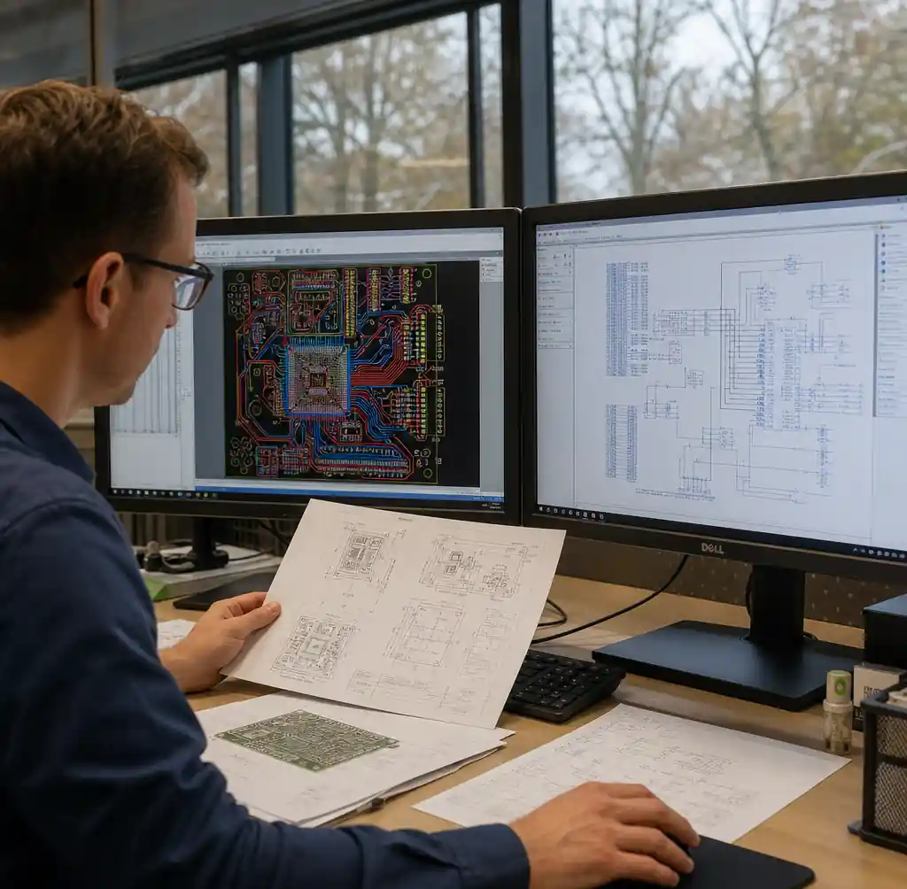
Submit a complete data package with zero ambiguity: Gerber files or IPC-2581 with clearly labeled layers, NC drill file with plated and non-plated holes separated, fabrication drawing with stackup cross-section showing all layer thicknesses and materials, impedance requirements with trace width and spacing targets, surface finish specification, solder mask and silkscreen colors, and board outline with dimensions and tolerances.
Common DFM issues that delay production include trace width below manufacturer capability (requesting 3mil traces when minimum is 4mil), insufficient spacing between copper features causing potential shorts, annular ring violations where vias sit too close to pads, and missing or unclear impedance control requirements. Run DFM analysis before submission using your manufacturer’s capability table. Andwin Circuits supports down to 3mil trace and space for standard boards, with tighter tolerances available for HDI designs.
Specifying tighter tolerances than your application requires adds unnecessary inspection steps and cost. A consumer IoT device operating below 100 MHz does not need ±5% impedance control that medical imaging equipment demands. Match your tolerance specification to actual electrical requirements, referencing IPC-6012 Class 2 for standard products and Class 3 for high-reliability applications only when needed.
Testing and Inspection Requirements
Testing and inspection ensure quality but extend lead time when specifications exceed standard practice. Matching your test requirements to actual risk reduces inspection time without compromising reliability.
Electrical testing verifies every net for continuity and isolation using flying probe or fixture methods. Flying probe tests any design without tooling but runs slower (8-15 minutes per board), suitable for prototypes and low volume under 50 units. Fixture-based testing requires 3-5 days to build the test fixture but then tests each board in 30-90 seconds, economical above 100 units. For fastest prototyping, specify flying probe testing to avoid fixture lead time.
Visual inspection options range from operator visual check (fastest, 2-5 minutes per board) to automated optical inspection (AOI) at 5-10 minutes per board with higher defect detection. X-ray inspection for BGAs and hidden features adds another 10-20 minutes per board. Standard lead time includes basic visual and electrical testing. Adding AOI or X-ray inspection extends delivery by 1-2 days unless you confirm equipment availability when ordering.
For automotive or medical applications requiring IPC-6012 Class 3 or IPC-A-610 Class 3 workmanship standards, inspection time increases 50-100% compared to Class 2 consumer products because inspectors examine more features at higher magnification. Plan accordingly and specify the appropriate class for your application rather than defaulting to Class 3.
Communication and Approval Workflows
Cross-border manufacturing introduces time zone delays that can extend lead time by 1-3 days per communication cycle. Optimizing approval workflows and pre-approving decisions eliminates these delays.
Engineering questions typically arrive during Asian business hours (UTC+8) when US-based engineers are offline. A question sent at 2pm Shanghai time (1am EST) waits until 9am EST for response, then waits another 16 hours until 2pm Shanghai the next day for the engineer to act. That 24+ hour cycle repeats for every question. Reduce this by front-loading communication: request a pre-production engineering review call to discuss any ambiguities before the clock starts, provide detailed fabrication notes answering common questions, and designate a contact person available during overlap hours (early US morning, late Asia afternoon).
Pre-approve common substitutions and variations to avoid stopping production for minor decisions. Authorize the manufacturer to substitute equivalent copper foil brands, adjust board dimensions by ±0.5mm for panelization efficiency, and use functionally equivalent surface finish if your first choice faces delay. These pre-approvals keep production moving when small issues arise.
Assembly Lead Time Considerations
If your project includes PCB assembly beyond bare board fabrication, component sourcing becomes the dominant lead time factor. In 2025-2026, semiconductor lead times remained elevated with many MCUs and power management ICs at 12-20 weeks, directly impacting assembly schedules.
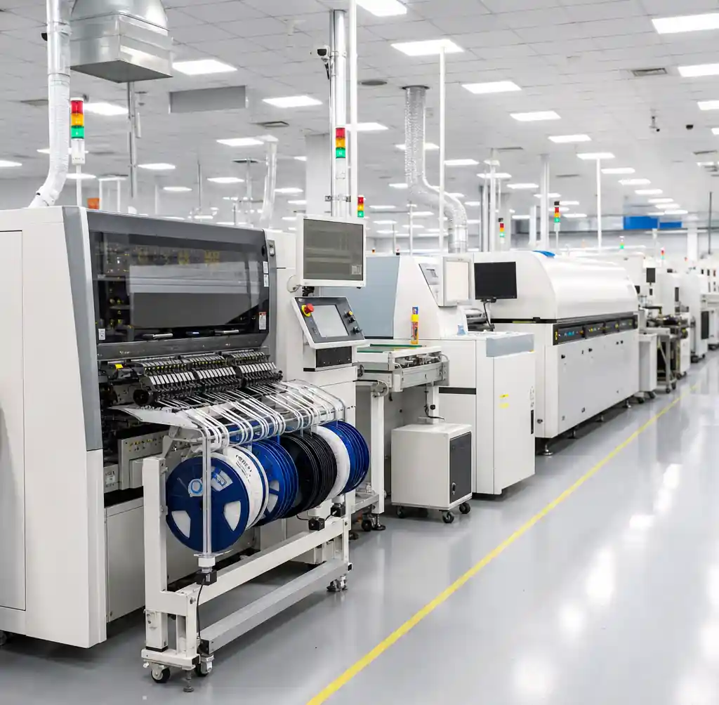
Turnkey assembly where the manufacturer sources all components offers convenience but adds component procurement time to your lead time. For a quick-turn assembly project, confirm all components are in stock before placing the order. Consigned assembly where you provide components gives you full control and can be faster if you pre-purchase long-lead items, but you own the shortage risk if any part is defective or arrives late.
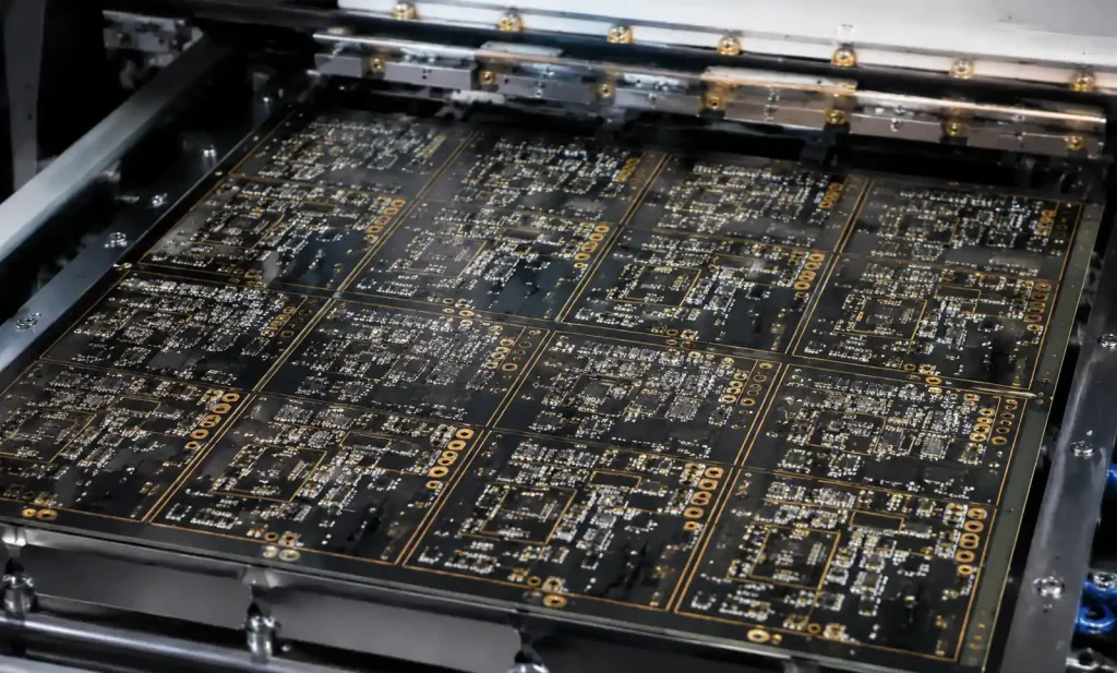
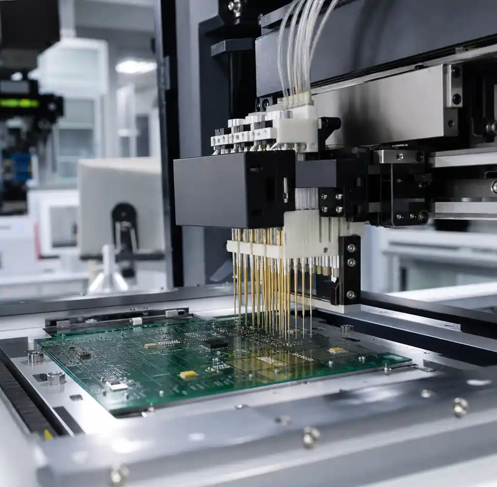
Low volume assembly typically requires 5-10 days including bare board fabrication, component kitting, SMT placement, reflow, and inspection. Adding conformal coating extends this by 1-2 days for application and curing.
Cost-Speed Trade-offs
Faster lead time costs more because it requires dedicated resources, lower panel utilization, and premium material sourcing. Understanding the cost curve helps you choose the optimal speed for each project phase.
Standard 15-20 day lead time provides baseline pricing. Cutting lead time to 10 days typically adds 15-25% cost premium. Quick-turn 5-7 day service adds 30-60% premium. Express 3-4 day service adds 60-100%+ premium. The premium covers dedicated equipment time, expedited material procurement, off-hours labor, and lower panel utilization efficiency.
The optimal strategy uses different lead times for different project phases. During initial prototyping with frequent design changes, pay the express premium to maximize iteration speed. After design validation when you’re building pre-production units, use standard lead time to control costs. For production ramps, plan 4-6 weeks ahead to use the most economical standard schedules. This phased approach balances speed and budget across the full development cycle.
FAQ
What is the fastest realistic lead time for a standard 4-layer PCB?
For a standard 4-layer FR-4 board with common materials and no special requirements, 3-5 days is achievable with quick-turn service. Standard lead time is 10-15 days.
Why does HDI PCB take longer than standard PCB?
HDI requires sequential lamination cycles and laser drilling of microvias, adding 3-5 days compared to standard through-hole construction. Each build-up layer requires separate processing steps.
How much does quick-turn service cost compared to standard?
Quick-turn premiums typically range from 30-60% for 7-day service up to 60-100%+ for 3-4 day express service. The premium covers dedicated equipment and lower panel utilization.
What causes the most common lead time delays?
Incomplete design files requiring engineering clarification cause the most delays, followed by material procurement for non-standard specifications. Component shortages dominate assembly lead time delays.
Can I reduce lead time for high layer count boards?
Layer count above 10 layers requires multiple lamination cycles that cannot be significantly compressed. Focus instead on confirming material stock and submitting clean files to avoid other delays.
Does surface finish choice affect lead time?
Yes. HASL and OSP apply fastest (2-4 hours), while ENIG requires 8-12 hours. Immersion silver and immersion tin fall between. For fastest prototyping, specify HASL or OSP unless flatness requirements demand ENIG.
Conclusion
PCB manufacturing lead time depends on design complexity, material availability, production scheduling, file quality, and communication efficiency. The fastest results come from designing to standard capabilities, confirming material stock before ordering, submitting complete DFM-verified files, and maintaining responsive communication during production.
Andwin Circuits offers PCB manufacturing from 4-50 layers with quick-turn service delivering in 7 days for standard specifications. Our facility maintains stock of common FR-4 materials, metal core substrates, and rigid-flex constructions to minimize procurement delays. We provide comprehensive DFM review and same-day engineering feedback to prevent schedule-impacting design issues.
Contact us for lead time optimization consultation, DFM analysis, and competitive pricing for your PCB project.