
PCB Assembly Failures: Solder Joint Issues and Rework Guidelines
Solder joint defects account for 55-70% of all PCB assembly failures in electronics manufacturing. From cold solder joints causing intermittent connections to tombstoning that lifts components off pads, these issues directly impact product reliability and customer satisfaction. According to IPC industry analysis, proper defect identification and rework procedures can reduce assembly failure rates by up to 80% while maintaining IPC-A-610 Class 3 quality standards.
This troubleshooting guide covers the most common solder joint defects in PCB assembly, their root causes, and professional rework procedures.
Common Solder Joint Defects
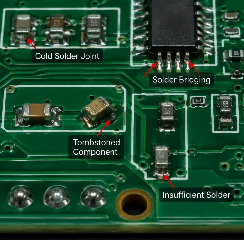
The table below compares the most common solder joint defects you will encounter in SMT and through-hole assembly processes.
| Defect Type | Visual Characteristics | Electrical Impact | Primary Cause |
|---|---|---|---|
| Cold Solder Joint | Dull, grainy surface; poor wetting | Intermittent connection | Insufficient heat |
| Solder Bridging | Solder connecting adjacent pads | Short circuit | Excess solder paste |
| Tombstoning | Component standing vertically | Open circuit on one end | Uneven heating |
| Insufficient Solder | Incomplete pad coverage | High resistance | Under-dosing paste |
| Solder Balls | Small solder spheres on board | Potential shorts | Paste splattering |
Each defect requires specific rework approaches per IPC-7711/7721 rework standards to restore assembly integrity without damaging components or PCB substrates.
Cold Solder Joints
Cold solder joints form when solder does not reach proper reflow temperature (typically 217°C for SAC305 lead-free solder) or cools too quickly before completing the wetting process. The resulting joint has a dull, grainy appearance instead of the smooth, shiny surface characteristic of proper solder bonds.
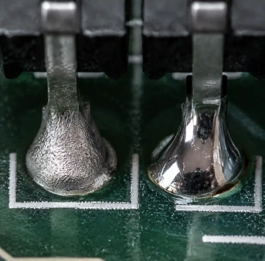
You will encounter this defect when reflow oven temperature profiles do not maintain adequate soak time (60-120 seconds at 150-180°C) or peak temperature falls below 235-245°C for lead-free solder. Manual soldering produces cold joints when operators use insufficient iron temperature (below 320°C) or remove the iron before solder fully wets the pad.
Remove the defective component using hot air or soldering iron at 340-380°C for lead-free. Clean pads with isopropyl alcohol (IPA) and apply fresh flux. Preheat the assembly to 100-120°C, then apply heat to both pad and lead simultaneously until solder reflows (2-4 seconds). Inspect the reworked joint under magnification to verify smooth, shiny appearance per IPC-A-610 acceptance criteria.
Solder Bridging
Solder bridging occurs when excess solder creates unintended electrical connections between adjacent pads, leads, or traces, causing short circuits that prevent proper circuit operation.
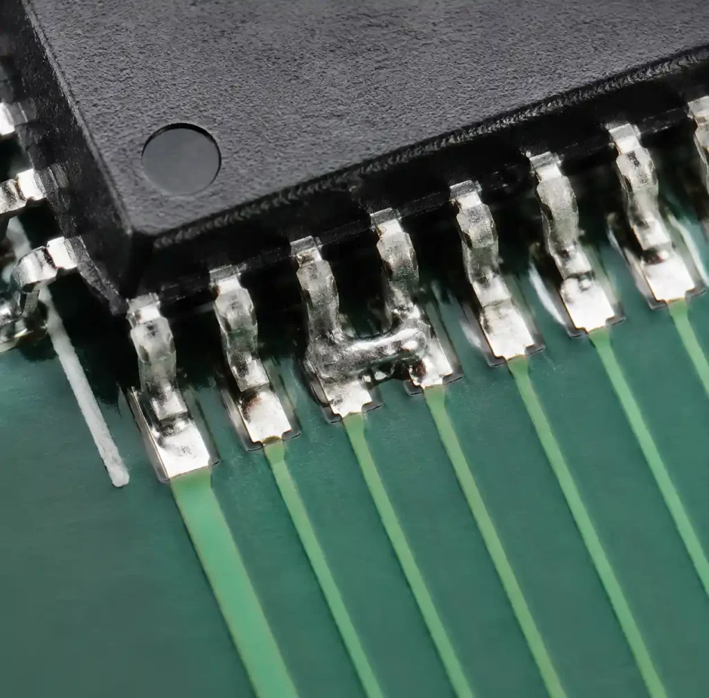
Excessive solder paste volume is the primary cause. You will see this issue when stencil aperture openings exceed optimal size (typically 1:1 ratio), paste printing pressure is too high, or component placement misalignment occurs. Fine-pitch components below 0.5mm pitch are particularly susceptible.
Use solder wick (desoldering braid) with fresh flux to remove excess solder. Position the wick between bridged pads and apply soldering iron (340-360°C) until solder wicks into the braid. Alternatively, use a fine-tip soldering iron to carefully drag excess solder away while applying flux. Verify isolation between adjacent pads using multimeter (>1 megohm resistance for isolated nets).
Tombstoning Defect
Tombstoning occurs when one end of a passive SMD component lifts vertically off its pad during reflow while the opposite end remains attached, creating an open circuit.
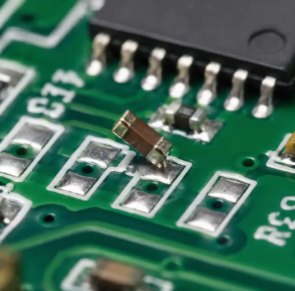
Tombstoning results from unbalanced wetting forces during solder reflow. You will encounter this defect when thermal gradients cause one pad to reach reflow temperature before the other. Component packages smaller than 0603 are most susceptible. Pad design asymmetry including unequal pad sizes or different copper areas creates thermal imbalance.
Ensure symmetrical pad geometry with equal length, width, and copper connection width for both component terminations. Maintain component placement accuracy within ±0.1mm. For rework, remove tombstoned components by applying hot air simultaneously to both pads. Clean pads with IPA, apply equal amounts of fresh solder paste to both pads, and place new component centered. Use hot air at 340-360°C with heat applied evenly to both terminations.
Insufficient Solder
Insufficient solder defects occur when solder volume is inadequate to form proper mechanical and electrical connections between component leads and PCB pads.
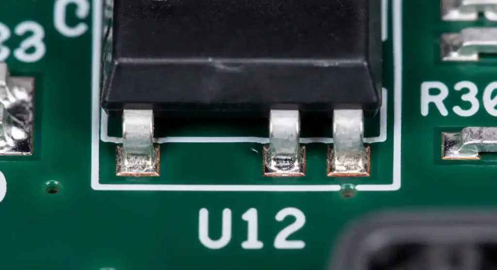
Visual inspection reveals incomplete solder coverage on pads, with exposed copper visible around component leads. Through-hole joints show insufficient barrel fill (below 75% per IPC-A-610 Class 2/3). Insufficient solder paste volume from under-printing is the primary cause when stencil apertures are undersized (below 0.8:1 ratio to pad area) or printing pressure is too low.
For SMD components, add flux to the defective joints and apply additional solder using fine solder wire (0.5-0.8mm diameter) with soldering iron. Heat the pad and component lead simultaneously while feeding small amounts of solder until proper fillet forms. For through-hole joints, apply flux to both sides and solder from the solder side while heating the component side.
Solder Balls and Splattering
Solder balls are small spheres of solidified solder that scatter across the PCB surface during reflow, creating potential short circuit risks.
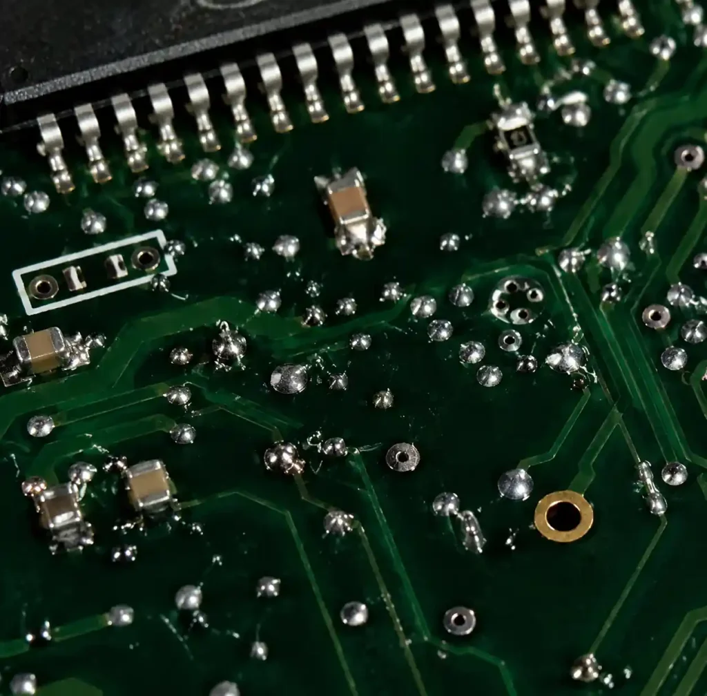
Solder balls form when volatile flux components vaporize rapidly, ejecting small solder particles. You will see increased formation with excessive reflow ramp rates (above 3°C/second) or inadequate soak time (below 60 seconds). Optimize reflow profile with gradual ramp rate (1-2°C/second), adequate soak zone (60-90 seconds at 150-180°C), and controlled peak temperature (240-250°C for SAC305). Remove solder balls using lint-free cleaners with IPA. For critical Class 3 assemblies, implement conformal coating after cleaning.
Inspection Methods
Effective defect detection requires multiple inspection techniques matched to assembly complexity.
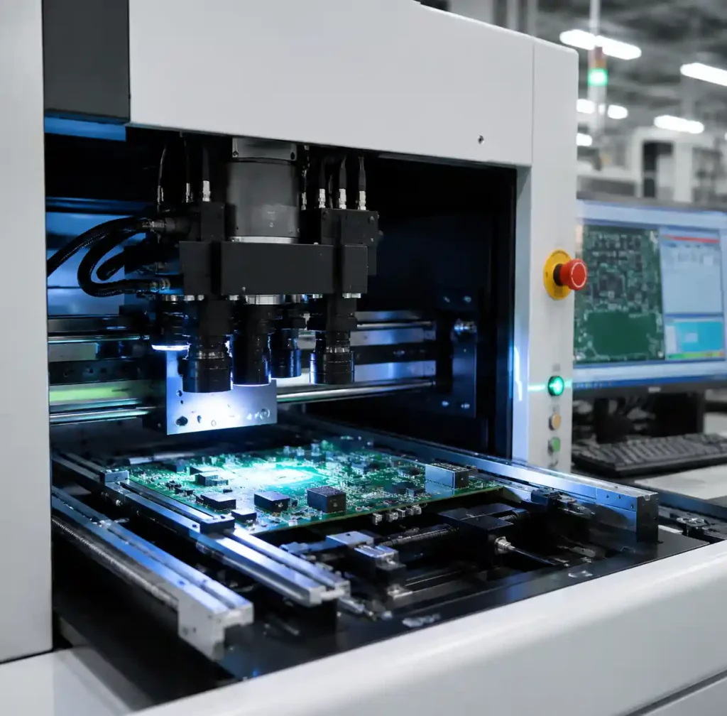
Manual visual inspection under magnification (10-30x stereoscope) identifies obvious defects including bridging and component misalignment. Automated Optical Inspection (AOI) systems use high-resolution cameras to capture solder joint geometry, identifying defects with 95-98% detection rates. You should implement AOI immediately post-reflow.
X-ray inspection reveals internal joint structure invisible to optical methods, essential for BGA, QFN, and components with hidden connections. IPC-A-610 standards specify maximum void content of 25% for Class 3 assemblies. In-circuit test (ICT) detects opens, shorts, and incorrect component values, achieving 98-99% defect coverage for accessible test points.
Professional Rework Guidelines
Professional rework restores defective assemblies to IPC-A-610 acceptance criteria without causing secondary damage. Following IPC-7711/7721 standards ensures consistent quality.
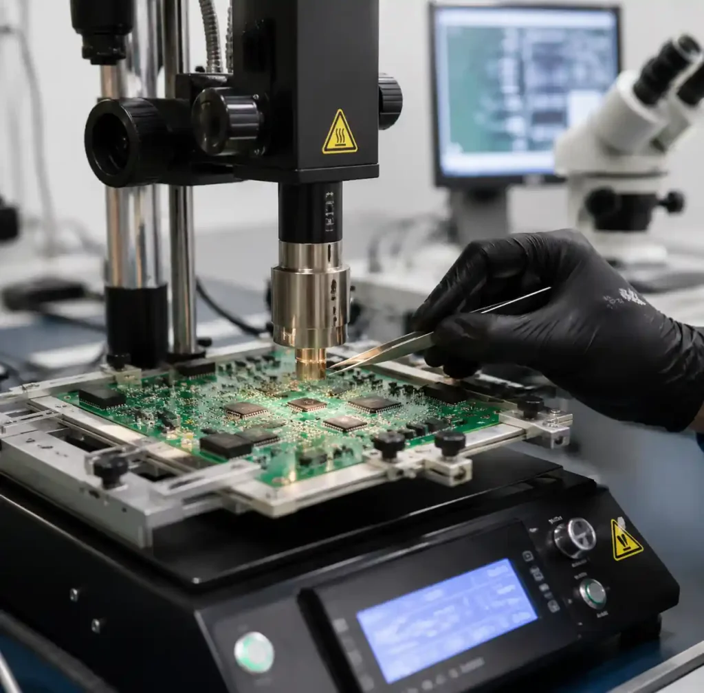
Essential equipment includes temperature-controlled soldering stations (±5°C accuracy), hot air rework stations with interchangeable nozzles, desoldering tools, and ESD-safe work surfaces. Support tools include flux dispensers, isopropyl alcohol (99% purity), lint-free wipes, and magnification equipment (10-40x). Calibrate temperature measuring equipment monthly.
For SMD components below 10mm, use soldering iron or hot air at 340-380°C depending on component thermal mass. Apply heat to all terminations simultaneously until solder reflows, then lift component with vacuum pickup. Clean pads thoroughly with IPA and inspect for damage. Apply fresh flux, place component with proper alignment, preheat to 100-120°C, then apply focused heat until solder reflows.
Prevention Strategies
Preventing solder joint defects through design optimization and process control eliminates costly rework.
Implement DFM rules during PCB layout including adequate pad sizes (1.2:1 ratio to component land pattern), proper solder mask clearance (0.05-0.1mm), and symmetric pad designs. Maintain minimum spacing between pads (0.15mm for 0.5mm pitch components) to prevent bridging. Work with your quick turn PCB assembly partner during design review.
Maintain solder paste printing quality through regular stencil inspection. Verify paste height (0.1-0.15mm) using solder paste inspection (SPI) systems. Optimize reflow profiles using profiling equipment. Target gradual ramp rates (1-3°C/second), adequate soak time (60-90 seconds), and peak temperature 20-30°C above liquidus.
| Prevention Strategy | Implementation | Expected Impact |
|---|---|---|
| DFM Review | Pre-production validation | 30-50% defect reduction |
| SPI Implementation | Automated paste inspection | 40-60% print defect reduction |
| Profile Optimization | Thermal profiling | 25-40% reflow defect reduction |
| AOI System | Post-reflow inspection | 95%+ detection rate |
FAQs
What causes most solder joint failures in PCB assembly?
Cold solder joints and insufficient solder account for 35-40% of all failures, followed by bridging (20-25%) and tombstoning (15-20%). These defects result from inadequate reflow temperature profiles, incorrect solder paste volume, or thermal imbalance. Proper process control including SPI, optimized reflow profiles, and AOI inspection reduces defect rates by 60-80%.
How do you identify a cold solder joint?
Cold solder joints display characteristic dull, grayish appearance with rough texture. Under 10-30x magnification, you will observe incomplete wetting at pad-lead interfaces and micro-cracks. Electrical testing shows higher contact resistance (>50 milliohms) or intermittent connections. X-ray inspection reveals incomplete intermetallic compound formation per IPC-A-610 acceptance criteria.
What temperature should I use for lead-free solder rework?
Use 340-380°C soldering iron tip temperature for SAC305 lead-free solder depending on component thermal mass. Larger components and metal core PCB assemblies require higher temperatures. Hot air rework should follow controlled temperature profile with peak temperature 240-250°C and adequate preheat to prevent thermal shock.
How can I prevent tombstoning in 0402 components?
Ensure symmetrical pad design with equal length, width, and thermal connections. Maintain component placement accuracy within ±0.1mm. Verify consistent solder paste volume (60-80% pad coverage) on both pads using SPI. Optimize reflow profile with gradual ramp rate (1-2°C/second) and adequate soak time (60-90 seconds) to minimize thermal gradients.
What is the difference between IPC-A-610 Class 2 and Class 3?
Class 2 covers general electronics where continued performance is desired but not critical. Class 3 applies to high-reliability electronics including medical devices, aerospace, and military applications. Class 3 requires tighter acceptance criteria including minimum 75% through-hole barrel fill (vs 50% Class 2) and more restrictive limits on voids and bridging.
Conclusion
Understanding common solder joint defects and implementing proper inspection and rework procedures is essential for reliable PCB assembly quality. Systematic prevention through DFM optimization, process control, and quality inspection reduces defect rates significantly while maintaining IPC-A-610 Class 3 standards.
If you need reliable PCB assembly services with rigorous quality control, Andwin Circuits provides turnkey assembly from prototypes to production volumes. Our facility maintains IPC-A-610 Class 3 inspection standards, ISO 9001 and IATF 16949 certification, and advanced inspection equipment including AOI and X-ray systems. We support complex assemblies up to 50 layers with fast delivery in 7-10 days.
Contact us today for PCB assembly quotes, technical consultation, or to discuss your specific quality requirements.