
How to Read PCB Capability Table: Understanding Manufacturer Specs
PCB capability tables account for nearly 40% of design-related issues in electronics manufacturing, with misinterpreted specifications responsible for production delays, increased costs, and failed prototypes. Understanding how to properly read and apply manufacturer capability specifications directly impacts your project timeline, budget, and final product quality.
If you want to design PCB projects that manufacturers can actually build within your requirements, then you will need to understand capability table parameters, tolerance interpretation, and design matching strategies.
This guide explains how to decode PCB capability tables, interpret critical parameters like trace width, spacing, hole sizes, and layer count, and match your design requirements to manufacturer specifications.
What Is a PCB Capability Table?
A PCB capability table is a technical specification document published by PCB manufacturers that lists the minimum and maximum fabrication parameters their production equipment can achieve. This document defines physical limits for trace widths, spacing, hole sizes, layer counts, board dimensions, copper weights, and material options.
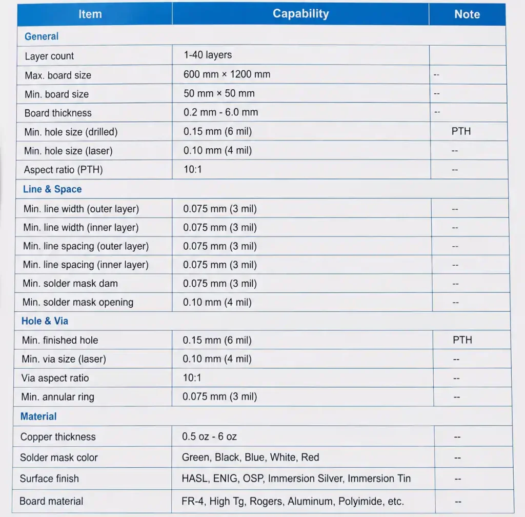
Capability tables serve as boundary conditions between your PCB design and what’s physically manufacturable. These specifications are based on the manufacturer’s equipment precision, process control capabilities, and IPC standard compliance levels.
You can use capability tables to validate design requirements before fabrication, identify which manufacturers can meet your specifications, and optimize designs for cost and lead time by staying within standard capabilities.
Key Parameters in PCB Capability Tables
Minimum Trace Width and Spacing
Trace width and spacing represent the most critical design parameters in any capability table. Minimum trace width defines the narrowest copper conductor a manufacturer can reliably etch, while minimum spacing indicates the smallest gap between adjacent copper features.
Standard manufacturers typically offer 5-6mil (0.125-0.150mm) trace and space capabilities, while advanced facilities can achieve 3-4mil (0.075-0.100mm) or finer features. HDI manufacturers with laser direct imaging (LDI) equipment often support 3mil or even 2mil features for high-density designs.
The relationship between trace width and copper weight matters significantly. Thicker copper makes fine features more challenging because etching must remove more material while maintaining edge definition.
| Capability Level | Min Trace/Space | Copper Weight | Typical Application | Cost Impact |
|---|---|---|---|---|
| Standard | 5/5 mil (0.125mm) | 1oz | Consumer electronics | Baseline |
| Advanced | 4/4 mil (0.100mm) | 0.5-1oz | Smartphones, tablets | +15-25% |
| HDI | 3/3 mil (0.075mm) | 0.5oz | Wearables, medical | +30-50% |
| Ultra-HDI | 2/2 mil (0.050mm) | 0.5oz | Advanced RF, high-speed | +60-100% |
Hole Size and Aspect Ratio
Hole size specifications define mechanical drill and laser drilling options. Minimum finished hole size ranges from 0.15mm to 0.20mm for mechanical drilling, while laser-drilled microvias achieve 0.10mm or smaller for HDI constructions.
Aspect ratio represents thickness divided by hole diameter. Standard manufacturers support 8:1 to 10:1 ratios—a 1.6mm board can have 0.20mm holes. Advanced facilities support 12:1 or higher.
For thick boards (3.0mm+), use larger holes or buried/blind vias to maintain platable aspect ratios.
Layer Count and Stack-up Options
Layer count capabilities vary significantly between manufacturers. Standard facilities support 2 to 16 layers, while advanced manufacturers offer 20 to 50+ layers. Andwin Circuits provides manufacturing up to 50 layers with controlled impedance and HDI features.
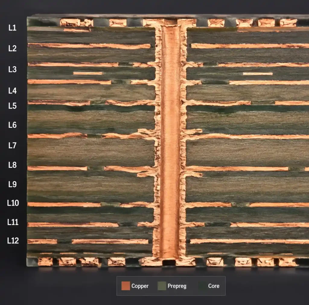
Manufacturers publish standard stack-up configurations for common layer counts (4L, 6L, 8L, 10L) that optimize signal integrity and power distribution. Understanding the manufacturer’s standard stack-up library helps you design within proven configurations, reducing manufacturing risk.
| Layer Count | Standard Stack-up | Applications | Lead Time | Registration Tolerance |
|---|---|---|---|---|
| 2-4 Layer | Signal-GND-PWR-Signal | Simple devices | 5-7 days | ±0.075mm |
| 6-8 Layer | S-G-S-S-P-S-G-S | High-speed digital | 7-10 days | ±0.075mm |
| 10-16 Layer | Complex multi-signal | Servers, telecom | 12-15 days | ±0.050mm |
| 20-50 Layer | Custom HDI | Aerospace, medical | 15-25 days | ±0.050mm |
Material Options and Thermal Properties
PCB capability tables specify available substrate materials, copper foil types, and dielectric options. Standard FR4 with Tg (glass transition temperature) from 130°C to 180°C remains most common.
High-frequency designs require specialized materials like Rogers, Taconic, or PTFE-based laminates. Metal core substrates provide thermal management for LED and power electronics. Flexible polyimide materials enable rigid-flex and flex circuit constructions.
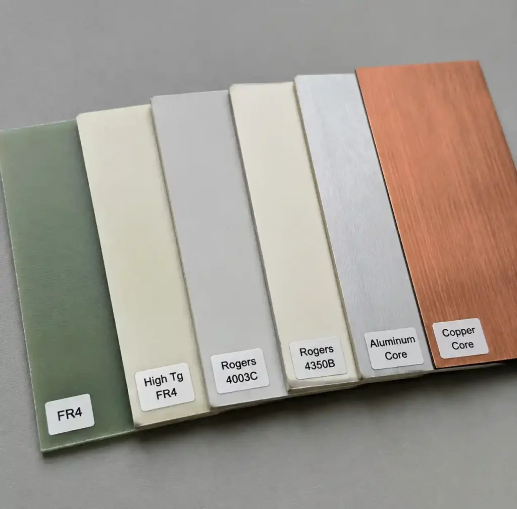
Verify material availability before finalizing specifications, as lead times for specialty materials can add 2-4 weeks.
Understanding Tolerance and Manufacturing Limits
Standard vs Advanced Capabilities
Most manufacturers publish two capability levels: standard capabilities for regular production and advanced capabilities requiring special processes. Standard capabilities represent what facilities manufacture consistently with high yields (95-98%) and short lead times (5-10 days).
Designing within standard capabilities delivers 20-40% cost savings and 30-50% faster lead times. Evaluate whether your design truly requires advanced capabilities or can be optimized to meet standard specifications.
IPC Standards and Quality Classes
PCB capability tables reference IPC standards that define quality requirements and acceptance limits. IPC-6012 covers rigid PCB qualification with three quality classes:
IPC Class 2 (General Electronic Products): Standard quality for consumer electronics and general-purpose equipment. Accepts minor cosmetic imperfections that don’t affect functionality.
IPC Class 3 (High Reliability Electronic Products): Enhanced requirements for medical devices, aerospace, and safety-critical systems. Class 3 specifies tighter tolerances and stricter acceptance criteria, adding 25-50% to costs.

Most consumer and industrial products function reliably at Class 2, while only safety-critical applications genuinely require Class 3 compliance.
How to Match Your Design to Manufacturer Capabilities
Design Rule Verification Process
Import capability table specifications into your PCB CAD tools as design rule constraints. Design rule checking (DRC) validates your layout against manufacturer limits in real time.
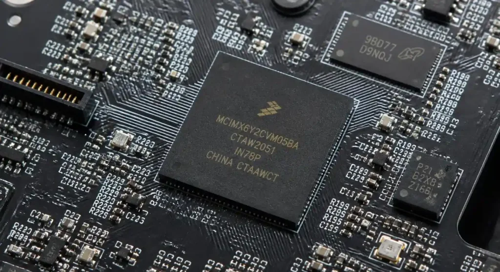
Pay special attention to high-density areas around fine-pitch components like BGAs and QFNs. These regions often require the smallest traces and vias.
Component Selection and Footprint Validation
Component selection directly impacts manufacturability. Fine-pitch components with 0.4mm or smaller pad spacing often require 3-4mil traces and smaller vias. Standard 0.5mm pitch BGAs route with 5mil traces and 0.20mm vias, while 0.4mm pitch devices may require HDI features.
Work with your manufacturer’s DFM team to review component selections before finalizing the design.
Cost Optimization Through Capability Alignment
Aligning your design with standard manufacturer capabilities delivers significant cost savings and faster turnaround. Each advanced feature adds 10-30% to costs and extends lead time by 2-5 days.
Trace Width: Widening from 4mil to 5mil moves designs into standard capability. Most digital signals under 100MHz work with 5-6mil traces.
Via Size: Increasing via diameter from 0.15mm to 0.20mm may eliminate HDI requirements.
Layer Count: Careful routing can reduce layer count by one or two layers, delivering 15-25% cost savings.
Material Selection: Standard FR4 with Tg 150-170°C meets most requirements. Specialty materials cost 3-10× more.
PCB Capability Parameters Explained
Copper Weight and Current Capacity
Copper weight defines foil thickness: 0.5oz (17μm), 1oz (35μm), 2oz (70μm), or heavy copper up to 6oz (210μm). Copper weight affects current capacity and thermal management.
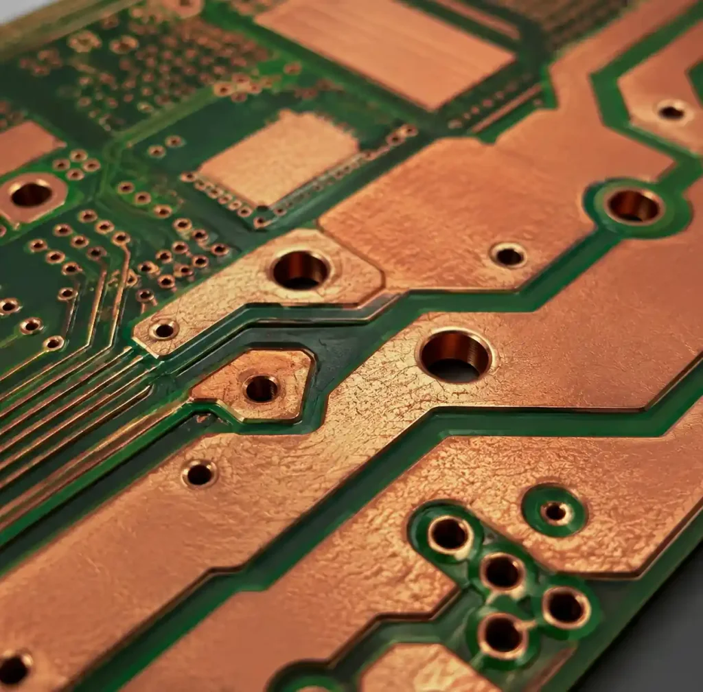
Most signal traces use 0.5-1oz copper, while power distribution requires 2oz or heavier. Calculate current requirements using IPC-2221 formulas.
Surface Finish Options and Compatibility
Surface finish options prevent oxidation and enable reliable soldering:
HASL: Standard finish with low cost but uneven surface. Not suitable for fine-pitch components.
ENIG: Flat surface ideal for fine-pitch components. Excellent for SMT assembly.
OSP: Thin coating with lowest cost. Limited shelf life (6-12 months), suitable for quick-turn prototypes.
Immersion Silver: Flat finish with good solderability. Moderate shelf life, good for RF applications.
Impedance Control and Testing
Impedance control specifications define the manufacturer’s ability to achieve target characteristic impedance for high-speed signals. Capability tables specify tolerance levels (±5%, ±10%) and testing methods.
Standard impedance control achieves ±10% tolerance, while advanced ±5% tolerance adds 15-25% to costs.
Provide detailed impedance requirements including target values during design submission.
Industry Applications and Standards Compliance
Automotive and Medical Requirements
Automotive PCB manufacturing requires IATF 16949 compliance and AEC-Q100 qualification. Capability tables specify extended temperature ranges (-40°C to +125°C or higher) and enhanced reliability testing. Medical device PCBs must meet ISO 13485 standards and typically require IPC Class 3 manufacturing.
Andwin Circuits holds ISO 9001, IATF 16949, and UL certifications, supporting automotive, medical, and industrial applications. Our manufacturing capabilities up to 50 layers and fast delivery in 7 days serve these demanding industries.
Telecommunications and High-Frequency PCBs
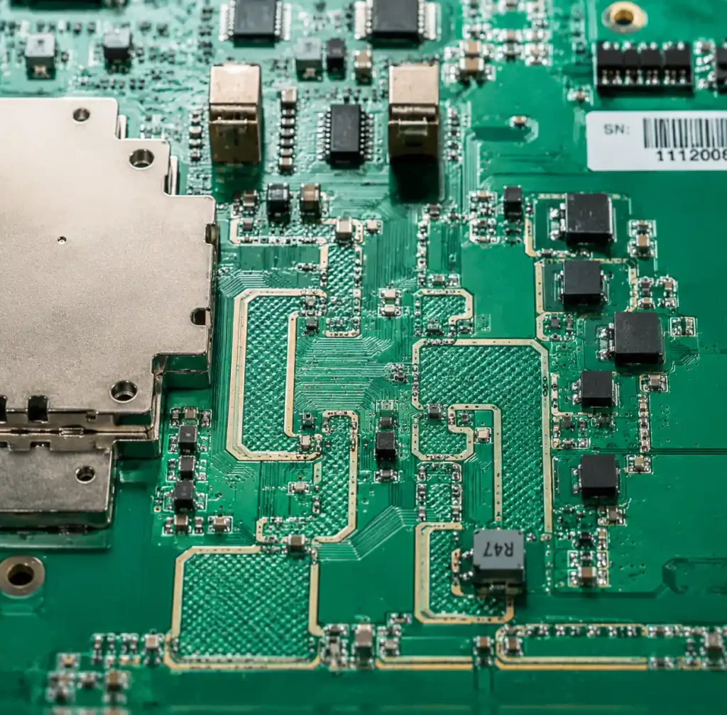
Telecommunications and 5G infrastructure require specialized high-frequency materials with controlled dielectric properties and low loss tangent. Capability tables for RF applications specify supported materials (Rogers, Taconic, PTFE), impedance control precision, and test frequencies.
Frequently Asked Questions
What is the difference between standard and advanced PCB capabilities?
Standard capabilities represent parameters a facility achieves consistently with high yields and short lead times (5-10 days). Advanced capabilities require specialized equipment and tighter controls, adding 20-50% to costs and 3-7 days to lead time.
How do I know which IPC class my project requires?
IPC Class 2 suits most consumer electronics and commercial products. IPC Class 3 is required for safety-critical applications in medical devices, aerospace, and automotive safety components. Unless regulatory requirements demand Class 3, Class 2 provides excellent reliability at lower cost.
What aspect ratio should I target for PCB vias?
Standard manufacturers support 8:1 to 10:1 aspect ratios. A 1.6mm thick board should use minimum 0.20mm via diameter. For thick boards (2.5mm+), consider buried or blind vias.
Can I mix different copper weights in one PCB design?
Yes, many manufacturers support mixed copper weights where signal layers use 0.5-1oz copper while power planes use 2-4oz heavy copper. This adds 10-20% to costs but optimizes performance.
How much does impedance control add to PCB cost?
Impedance control with ±10% tolerance adds 15-25% to costs. Tighter ±5% tolerance may add 30-40%. However, impedance control is essential for signal integrity in high-speed digital (>50MHz) and RF applications.
What minimum trace width should I use for power distribution?
Use IPC-2221 calculations. For 1oz copper with 10°C temperature rise: 100mA needs 5mil width, 1A requires 20mil, 3A needs 80mil. Verify calculated widths against manufacturer capabilities.
Conclusion
Understanding PCB capability tables directly impacts your product development success, manufacturing costs, and time to market. This guide covered critical parameters including trace width, spacing, hole sizes, layer counts, and tolerance requirements that define reliable production capabilities.
If you need high-quality PCB manufacturing for your electronic device project, Andwin Circuits offers advanced capabilities up to 50 layers with fast turnaround in 7 days. Our facility is certified to ISO 9001, IATF 16949, and UL standards, ensuring superior quality for automotive, medical, telecommunications, and IoT applications.
Contact us today for custom PCB solutions and competitive factory-direct pricing.