
PCB Thermal Via Design: Spacing, Diameter, and Fill for Heat Transfer
When you’re pushing 5W through a QFN-32 package on a 1.6mm FR-4 board, the difference between a properly designed thermal via array and a poorly executed one can mean 20-30°C at the junction. After reviewing hundreds of thermal failures in production, I’ve seen that most thermal management problems stem from three interconnected variables: via diameter, spacing, and fill strategy. Get these wrong, and you’re not just adding thermal resistance—you’re creating localized hotspots that cascade into reliability issues.
Why Thermal Via Geometry Drives Heat Transfer Performance
Thermal vias work by creating vertical copper columns that conduct heat from surface-mounted components down to internal ground planes or bottom-side heatsinks. Unlike signal vias that prioritize electrical connectivity, thermal vias maximize cross-sectional copper area and minimize the thermal resistance path.
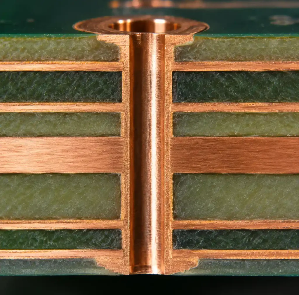
The effectiveness of your thermal via design depends on three critical parameters working together: the via diameter determines the copper cross-section available for conduction, the spacing between vias affects how efficiently heat spreads from the source pad, and the fill material (or lack thereof) influences both thermal conductivity and mechanical stability during assembly.
The Thermal Resistance Reality
A single 0.3mm diameter via through a 1.6mm board contributes approximately 30-40°C/W of thermal resistance. That might seem manageable until you calculate the total resistance from junction to ambient. With typical values of 5°C/W from junction to case, 1°C/W from case to board, and 15°C/W from board to ambient, every degree matters when you’re trying to keep junction temperatures below 125°C in a 70°C ambient.
Optimal Via Diameter Selection
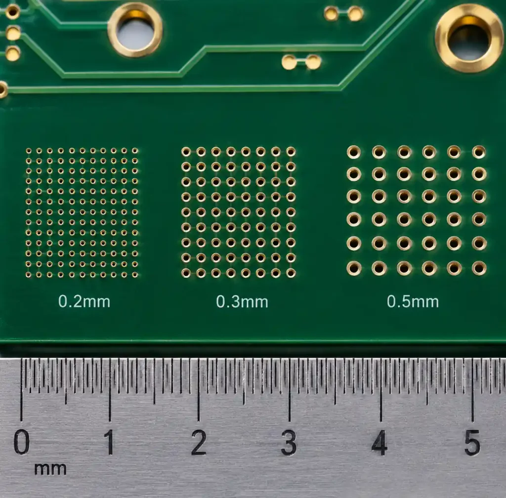
Via diameter directly impacts thermal conductivity, but it’s constrained by PCB thickness, manufacturing capabilities, and the available area under your thermal pad. The industry has converged on three diameter ranges based on application requirements.
| Via Diameter | Typical Application | Thermal Performance | Manufacturing Considerations |
|---|---|---|---|
| 0.2-0.25mm | Space-constrained QFNs, dense arrays | 40-50°C/W per via | Requires tight process control, higher cost |
| 0.3-0.35mm | Standard power devices, MOSFETs | 30-40°C/W per via | Industry standard, reliable manufacturing |
| 0.4-0.5mm | High-power applications, thermal pads >5x5mm | 20-30°C/W per via | Larger keepout zones, solder wicking risk |
For most applications, 0.3mm finished diameter (0.25mm drill) delivers the best balance. This size provides sufficient copper cross-section while remaining compatible with standard PCB fabrication processes that maintain 8:1 aspect ratios on 1.6mm boards.
Why Larger Isn’t Always Better
Increasing via diameter from 0.3mm to 0.5mm does improve the thermal conductivity of each individual via by approximately 25-30%. However, larger vias consume more pad real estate, reducing the total number you can fit under a thermal pad. For a 3x3mm QFN thermal pad, you might fit nine 0.3mm vias at standard spacing versus only four 0.5mm vias—resulting in worse overall thermal performance despite the better per-via conductivity.
Critical Spacing Rules for Thermal Via Arrays
Via spacing determines how effectively heat spreads from the component pad into the via array. Place vias too far apart, and you create thermal bottlenecks where heat must conduct laterally through FR-4 before reaching a via. Place them too close, and you risk mechanical weakness, solder wicking during reflow, and increased manufacturing costs.
The generally accepted spacing rule is 1.2-1.5 times the via diameter, measured center-to-center. For 0.3mm vias, this translates to 0.36-0.45mm spacing. However, this rule requires context-dependent adjustment.
Edge Distance and Pad Coverage
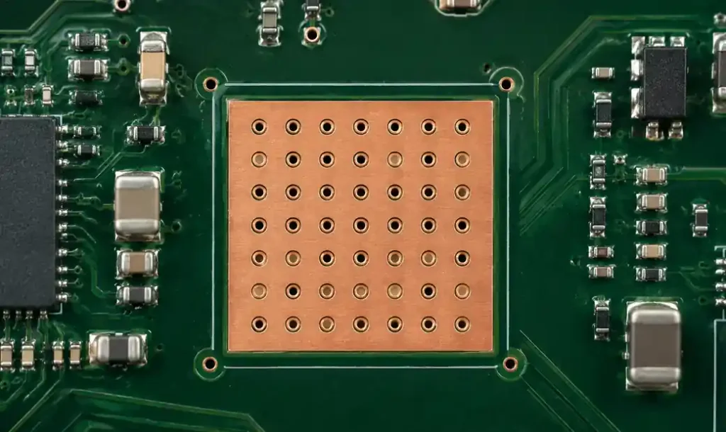
Vias should be positioned at least 0.15mm from the edge of the thermal pad to prevent solder wicking during reflow. This edge clearance becomes critical for smaller packages. On a 3x3mm thermal pad with 0.15mm edge clearance, your effective via placement area shrinks to 2.7×2.7mm—a 19% reduction in available space.
The optimal pattern places vias in a grid array that maximizes coverage while maintaining minimum spacing. For rectangular thermal pads, this often means using a staggered pattern rather than a perfect grid to achieve better thermal uniformity.
| Thermal Pad Size | Recommended Via Count (0.3mm) | Pitch (Center-to-Center) | Expected Thermal Resistance |
|---|---|---|---|
| 3x3mm | 4-6 vias | 1.0-1.2mm | 8-12°C/W |
| 5x5mm | 9-12 vias | 1.2-1.4mm | 4-6°C/W |
| 7x7mm | 16-20 vias | 1.2-1.5mm | 2-3°C/W |
| 10x10mm | 25-36 vias | 1.5-1.8mm | 1-2°C/W |
Via Fill Strategies: When and What to Use
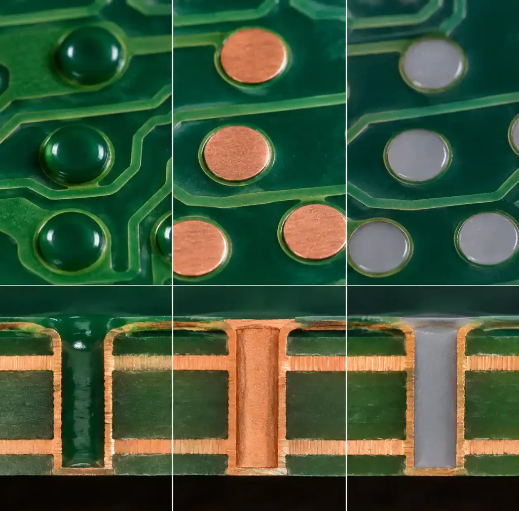
Via fill directly impacts three critical factors: solder wicking control during assembly, thermal conductivity enhancement, and mechanical pad support. The decision to fill, partially fill, or leave vias open depends on your component type, assembly process, and thermal requirements.
Unfilled (Tented) Vias
Tented vias use solder mask caps on both top and bottom to prevent solder from wicking into the via barrel during reflow. This approach works for components with moderate power dissipation (<2W) where the via copper plating alone provides adequate thermal conductivity. The copper plating thickness, typically 25-35µm, creates an annular ring of copper that conducts heat vertically.
The primary advantage of tented vias is cost—they require no additional process steps beyond standard PCB fabrication. The disadvantage is thermal performance: the hollow via barrel has an effective thermal conductivity roughly 30-40% lower than a copper-filled via due to the air gap in the center.
Copper-Filled Vias
Copper-filled vias use electroplating to completely fill the via barrel with solid copper, eliminating the air gap and maximizing thermal conductivity. This approach reduces thermal resistance by 25-35% compared to tented vias and provides excellent mechanical support for thermal pads during assembly.
The process requires via plugging with copper during PCB fabrication, followed by planarization to create a flat surface. This adds 2-3 days to manufacturing lead time and increases cost by approximately 15-25%. Copper fill becomes cost-effective for power devices exceeding 3W or when junction temperature margins are tight.
Epoxy-Filled Vias
Epoxy fill uses conductive or non-conductive epoxy to plug the via. Conductive epoxy (typically silver-filled) provides thermal conductivity between unfilled and copper-filled options—roughly 15-20% better than tented vias. Non-conductive epoxy primarily prevents solder wicking without significantly improving thermal performance.
Epoxy fill costs less than copper fill but requires an additional process step. Use it when solder wicking is your primary concern rather than maximum thermal performance.

Design Validation: Calculating Your Thermal Via Performance
Before committing to production, validate your thermal via design using the thermal resistance calculation method. The total thermal resistance from component to board consists of three series components: junction to case (from datasheet), case to board (contact resistance), and board spreading resistance (via array performance).
For via array performance, use this simplified calculation:
R_via = (ρ × L) / (n × A)
Where:
- ρ = copper thermal resistivity (0.0025 m·K/W)
- L = board thickness (e.g., 0.0016m for 1.6mm)
- n = number of vias
- A = copper cross-sectional area per via (π × r²)
For a 1.6mm board with twelve 0.3mm copper-filled vias:
- A = π × (0.00015)² = 7.07 × 10⁻⁸ m²
- R_via = (0.0025 × 0.0016) / (12 × 7.07 × 10⁻⁸) = 4.7°C/W
This simplified model ignores copper spreading resistance in the destination plane, which typically adds 1-2°C/W depending on plane size and thickness.

Common Design Mistakes to Avoid
After reviewing thermal failures across multiple product lines, these issues appear repeatedly:
Insufficient via count: Designers often underestimate the number of vias required. A 5W device on a 5x5mm pad needs at least 12-16 vias to achieve acceptable thermal resistance. Using only 6-8 vias might meet electrical requirements but creates thermal hotspots.
Ignoring destination plane size: Thermal vias don’t remove heat—they move it to a copper plane. If that destination plane is too small (<20x20mm for a 5W device), the spreading resistance dominates and adding more vias provides minimal benefit. Size your internal ground plane at least 4-5 times the thermal pad dimension in each direction.
Over-reliance on top-side copper: The 35µm copper foil on the top layer has minimal thermal mass. Don’t expect top-side copper pours to significantly reduce thermal resistance. The real thermal path goes through vias to thick internal planes or bottom-side copper.
Via placement under solder-excluded areas: Some QFN datasheets specify solder mask openings smaller than the physical thermal pad. Placing vias outside the solder mask opening but under the metal pad creates areas where solder cannot reflow properly, resulting in poor thermal contact.
Integration with Broader Thermal Management
Thermal via design works as part of a complete thermal management system. Your via array moves heat to internal copper planes, but those planes must connect to additional cooling mechanisms: increased copper weight, thermal interface materials, or external heatsinks.
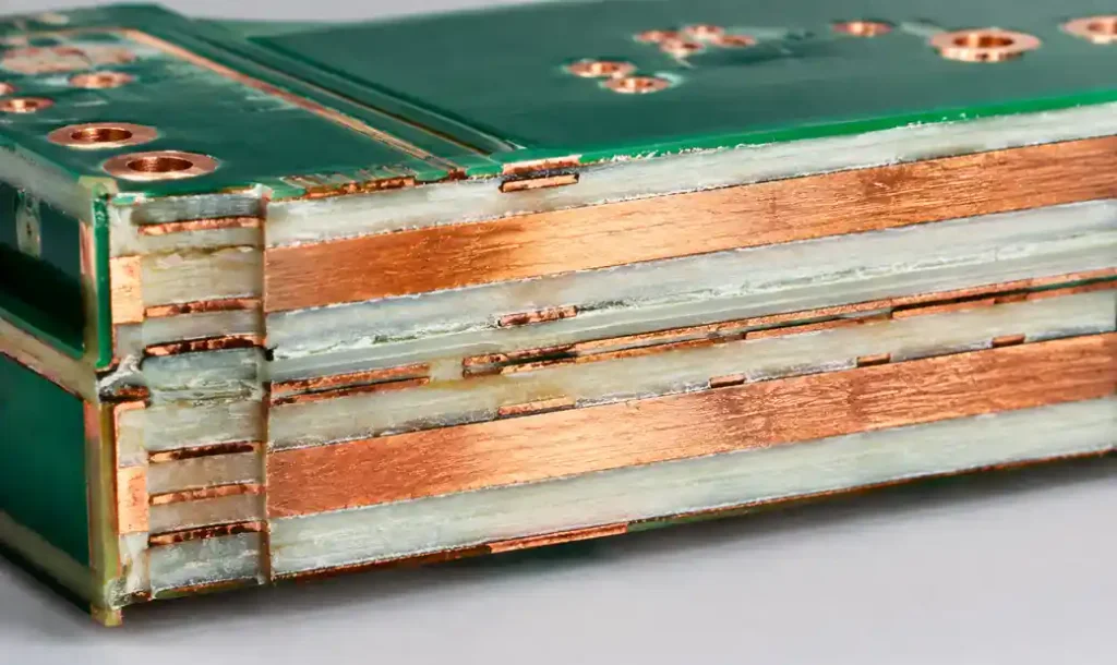
For multilayer boards, connect your thermal vias to the thickest internal copper planes available—typically 2oz (70µm) ground planes. Thin signal layers (17.5µm) provide inadequate thermal mass for heat spreading. If your stackup allows, dedicate an internal layer as a thermal plane with 3-4oz copper specifically for heat spreading.
Material Selection Impact
FR-4 has poor thermal conductivity (0.3-0.4 W/m·K) compared to aluminum (205 W/m·K) or copper (385 W/m·K). This fundamental limitation means that lateral heat spreading in FR-4 is inefficient—heat conducts much better through copper than through the board material. This is why via arrays must be densely packed under thermal pads rather than spread out across a large area.
For applications exceeding 10W, consider thermal management substrates like metal-core PCBs (MCPCBs) or ceramic materials that provide 10-20× better thermal conductivity than FR-4. In these materials, via design becomes less critical because lateral spreading is significantly more efficient.
Manufacturing Considerations and Cost Tradeoffs
Thermal via specifications directly impact PCB manufacturing cost and yield. While 0.3mm vias with standard tenting add minimal cost, copper-filled vias with planarization can increase board costs by 20-30%. Before specifying copper fill across your entire design, identify which components actually require it based on power dissipation.

Work closely with your PCB fabricator to understand their process capabilities. Some manufacturers struggle with aspect ratios above 8:1, limiting via diameter on thick boards. Others have optimized copper-fill processes that reduce cost premiums. Getting fabricator feedback during design prevents yield issues and expedited rework costs.
Via-in-Pad Reliability
Via-in-pad designs where vias sit directly under component pads require either filling or plugging to prevent solder wicking into the via barrel during reflow. Unfilled vias under solder pads create voids that weaken solder joints and degrade thermal contact. This failure mode appears as intermittent thermal issues that worsen over thermal cycling as the solder joint progressively degrades.
Plugging can use either copper or epoxy. Copper provides better thermal performance but costs more. Non-conductive epoxy prevents solder wicking at lower cost but adds minimal thermal benefit. Choose based on your thermal requirements and budget.
Real-World Application Guidelines
Based on power dissipation levels, here’s practical guidance for thermal via design:
<1W devices: Standard tented vias, 0.3mm diameter, 4-6 vias under thermal pad, 1.2mm pitch. This covers most small signal devices, low-power MOSFETs, and analog ICs.
1-3W devices: Tented or epoxy-filled vias, 0.3mm diameter, 8-12 vias, 1.0-1.2mm pitch. Connect to 2oz internal ground plane minimum 25×25mm. Typical applications include power MOSFETs, small voltage regulators, and interface ICs.
3-8W devices: Copper-filled vias required, 0.3-0.35mm diameter, 12-20 vias depending on pad size, 1.0-1.2mm pitch. Connect to 2-3oz internal plane >40×40mm. Consider additional top-side copper pour for lateral spreading. Applications include power management ICs, motor drivers, and RF power amplifiers.
>8W devices: Copper-filled vias, 0.35-0.4mm diameter, maximum via count limited by pad area, 1.2-1.5mm pitch. Requires 3-4oz internal thermal plane, potential external heatsink with thermal interface material, or migration to MCPCB substrate. This category includes high-current power supplies, RF power transistors, and processor thermal management.
FAQ
Q: Can I use the same via design for both signal routing and thermal management?
A: No. Signal vias prioritize electrical performance and are typically smaller (0.2-0.25mm) with wider spacing to accommodate trace routing. Thermal vias need larger diameter and denser spacing to maximize copper cross-sectional area. Use dedicated thermal via arrays under power components rather than relying on signal vias to conduct heat.
Q: How do I prevent solder from wicking into thermal vias during assembly?
A: Use solder mask tenting (solder mask caps over the via openings) for unfilled vias, or specify copper/epoxy filling during PCB fabrication. For via-in-pad designs, plugging is mandatory—unfilled vias under solder pads create voids that weaken joints and degrade thermal contact.
Q: What’s the minimum via spacing my PCB manufacturer can reliably produce?
A: Most standard fabricators handle 0.9-1.0mm via pitch (center-to-center spacing) with high yield. Tighter spacing (0.7-0.8mm) is possible but may require advanced fabrication capabilities and increases cost. Always verify capabilities with your specific manufacturer before finalizing designs.
Q: Should I use thermal vias on both sides of the board?
A: Only if you have active cooling (heatsink, airflow) on the bottom side. For standard installations where the bottom of the board faces a chassis or has no forced cooling, thermal vias should connect the top-side component to bottom-side copper planes that spread heat laterally. Adding vias from bottom to top just adds unnecessary thermal resistance unless there’s a specific cooling path.
Q: How does board thickness affect via thermal performance?
A: Thicker boards increase thermal resistance proportionally—a via through 2.4mm board has 50% higher resistance than the same via through 1.6mm board. For thick boards (>2.0mm), increase via diameter to 0.35-0.4mm to compensate, or use stacked microvias in HDI designs to reduce the effective thermal path length.
Q: Can I calculate thermal via performance accurately or do I need simulation?
A: Simple calculations using the formula in this article provide adequate accuracy (±15-20%) for initial design. For critical applications or complex geometries, use thermal simulation tools like Ansys Icepak or FloTHERM to account for copper spreading, board stackup variations, and boundary conditions. Always validate critical designs with thermal imaging during prototype testing.
Conclusion
Thermal via design requires balancing three interconnected variables: diameter, spacing, and fill method. Standard 0.3mm vias spaced at 1.2-1.5× diameter with copper fill for power >3W covers most applications. However, effective thermal management extends beyond via design—your via array must connect to adequately sized copper planes, and total system thermal resistance must account for junction-to-ambient heat flow.
Start your design by calculating the required thermal resistance from component datasheets and ambient conditions. Work backward to determine how many vias you need, then verify you can fit them under the available thermal pad with proper spacing and edge clearance. Validate with thermal calculations or simulation before committing to production, and always test prototypes with thermal imaging to confirm performance meets specifications. The most reliable thermal designs result from understanding the complete heat transfer path rather than simply following via design rules without context.