
PCB Thickness Selection: Standard vs Custom Thickness Trade-offs
PCB manufacturing specifications account for 35% of product development costs, with thickness selection directly impacting mechanical reliability, electrical performance, and production timelines. You will need to understand standard thickness options, custom requirements, cost implications, and application-specific considerations to make informed design decisions for your electronic products.
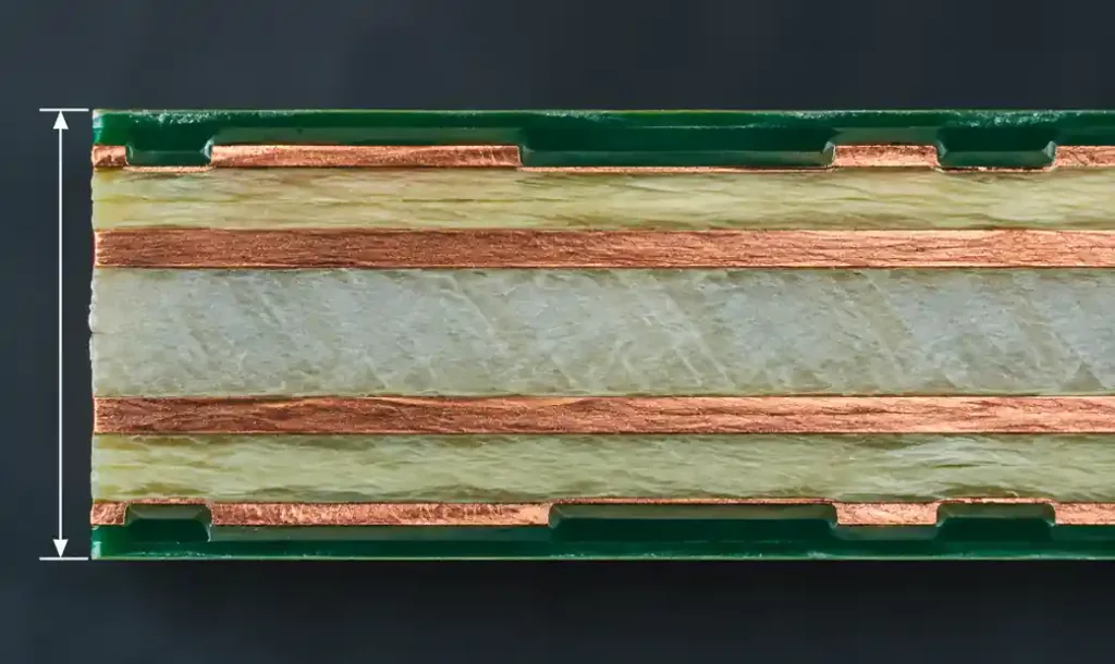
What Is PCB Thickness?
PCB thickness refers to the total height of the laminated circuit board structure, measured from top to bottom surface, including copper layers, dielectric materials, solder mask, and surface finish. Standard thickness is measured in millimeters or mils (1 mil = 0.0254 mm) per IPC-6012 specifications. The thickness consists of core layers, prepreg bonding material, copper foils, and surface coatings that provide structural integrity and design flexibility.
Standard PCB Thickness Options
1.6 mm (0.062 inch) – Industry Default
The 1.6 mm thickness dominates PCB manufacturing worldwide, accounting for approximately 60% of all commercial boards produced. This dimension provides optimal mechanical stiffness for through-hole component leads, fits standard PCB connectors and mounting hardware, and delivers cost-effective production with minimal lead time.
You can specify 1.6 mm PCB for consumer electronics, industrial controls, telecommunications equipment, and IoT devices where mechanical stability and component compatibility are essential. This thickness supports layer counts from 2 to 20+ layers and accommodates controlled impedance designs for high-speed signals up to 10 Gbps.
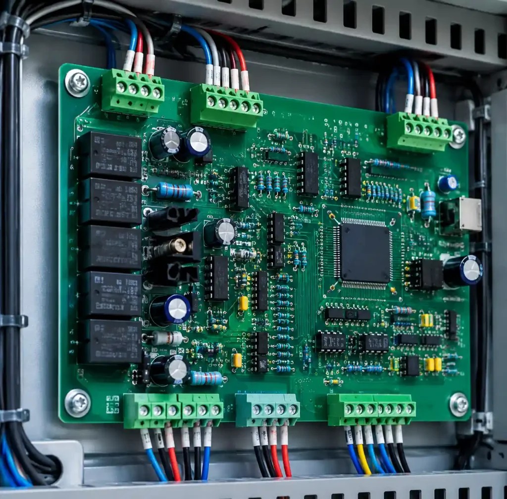
1.0 mm and 1.2 mm – Compact Applications
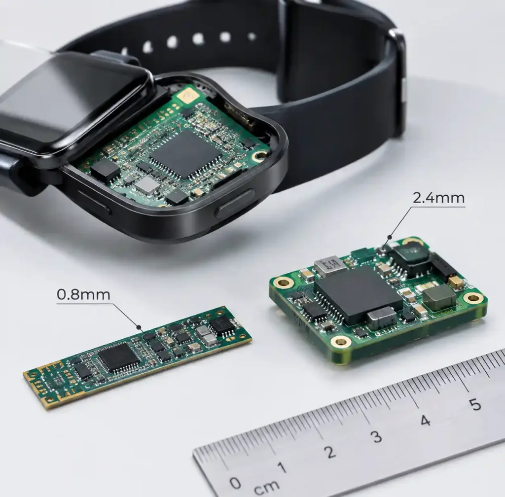
Thinner boards (1.0-1.2 mm) reduce weight and profile height for space-constrained products like mobile devices, wearables, and medical implantables. These PCBs require careful handling during assembly and may need support structures to prevent warping. Manufacturing considerations include reduced drill aspect ratio capability (typically 8:1 maximum), increased thermal stress susceptibility, and potential through-hole component challenges.
2.0 mm and 2.4 mm – High-Power Applications
Thicker PCBs provide enhanced mechanical strength, improved heat dissipation, and better support for heavy components. Power electronics, industrial controls, automotive power modules, and LED drivers often require 2.0-2.4 mm thickness for high current loads and thermal cycling. These boards allow larger drill holes, accommodate heavier copper weights (3-6 oz), and provide flexibility for complex multilayer stackups.
Standard vs Custom Thickness Comparison
| Parameter | Standard Thickness (1.6mm) | Custom Thickness (0.8-2.4mm) |
|---|---|---|
| Lead Time | 5-7 days | 10-15 days |
| Cost Premium | Baseline | +15% to +30% |
| Layer Count | 2-20+ layers | 2-12 layers (typical) |
| Min Drill Size | 0.2 mm | 0.25-0.3 mm |
| Aspect Ratio | Up to 12:1 | 8:1 to 10:1 |
| Tooling Availability | Immediate | Custom setup required |
How PCB Thickness Affects Mechanical Strength
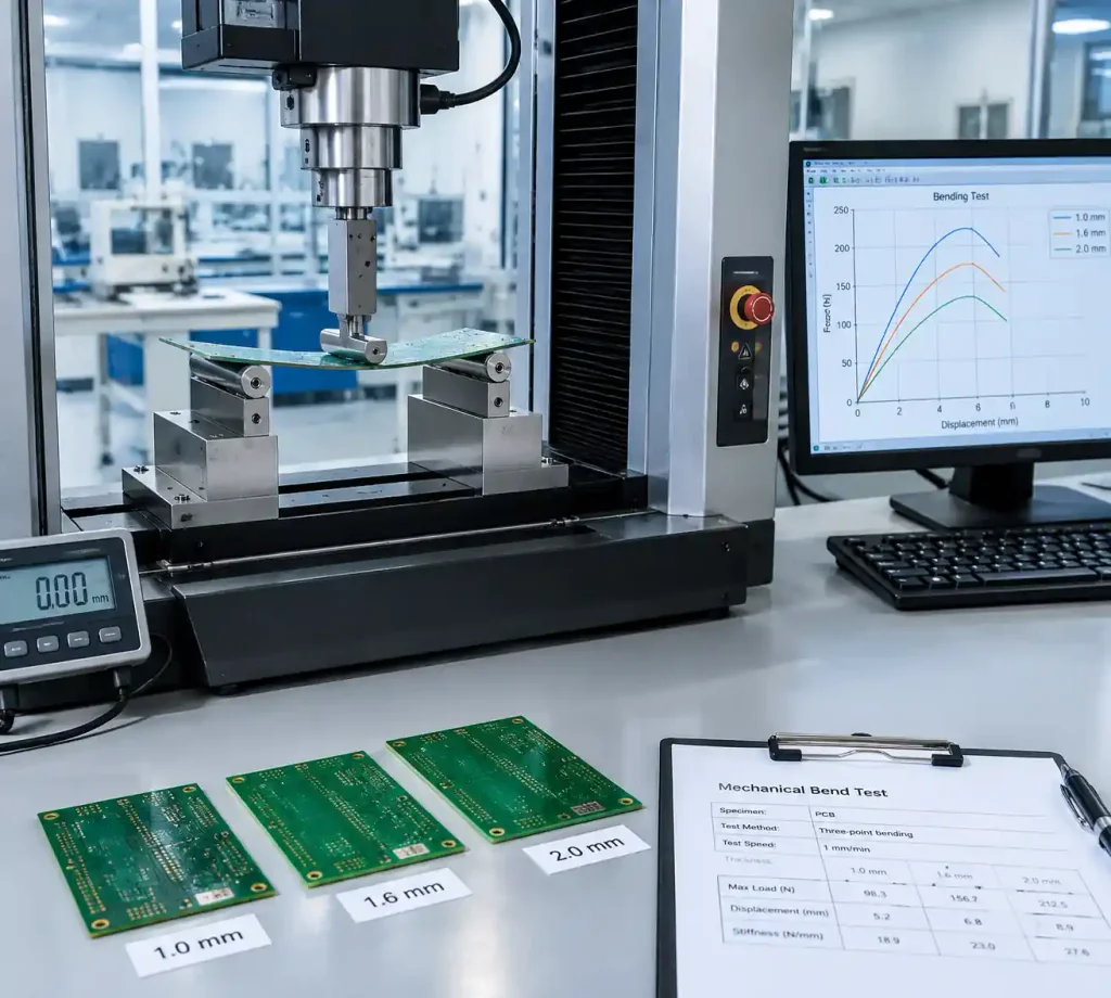
Board stiffness increases with the cube of thickness, meaning a 2.0 mm PCB is approximately 2.4 times stiffer than a 1.6 mm board. This mechanical property impacts resistance to bending stress, vibration tolerance, and warpage during thermal cycling per IPC-TM-650 test methods. Products exposed to vibration (automotive, industrial), thermal cycling (power electronics), or handling stress (consumer devices) require adequate stiffness to prevent solder joint failures. Support structures including ribs and mounting points can compensate for thinner boards, but fundamental mechanical strength derives from thickness selection matched to IPC-6012 Class requirements.
Impedance Control and Thickness Selection
Controlled impedance traces require precise dielectric thickness between signal layers and reference planes. Standard 1.6 mm boards with defined core and prepreg thicknesses enable reliable 50-ohm and 100-ohm impedance control with ±10% tolerance per IPC-2141. Custom thickness boards require detailed stackup analysis to achieve target impedances, potentially limiting layer options or requiring special materials. You should specify standard thickness when impedance control is critical for high-speed digital signals (DDR4, PCIe, USB 3.x), RF applications, or differential signaling.
PCB Thickness and Connector Compatibility
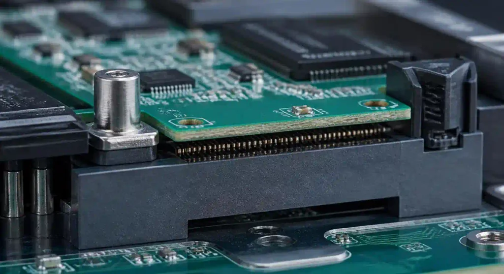
Edge connectors, card slots, and mezzanine connectors are designed for specific PCB thicknesses with mechanical tolerances of ±0.15 mm. PCI Express cards require 1.6 mm ±0.1 mm per PCI-SIG specifications, while memory modules specify 1.2 mm or 1.6 mm depending on form factor. Connector manufacturers provide retention force specifications based on nominal thickness. You must verify connector datasheets for thickness compatibility before finalizing board design, as custom thickness may require custom connectors with 4-8 week procurement lead times.
Cost Implications: Standard vs Custom Thickness
Standard thickness PCBs use readily available materials stocked by manufacturers, eliminating procurement delays and setup costs. Custom thicknesses require special material ordering, custom tooling, and modified processes, resulting in 15-30% cost premium and extended lead times. The cost differential becomes more significant for prototypes and low-volume production where setup costs dominate. High-volume production (1000+ units) amortizes setup costs, reducing the relative premium to 10-15%.
Cost Optimization Table
| Production Volume | Standard Thickness Cost | Custom Thickness Cost | Lead Time Difference |
|---|---|---|---|
| Prototype (1-10) | Baseline | +25-30% | +5-7 days |
| Low Volume (10-100) | Baseline | +20-25% | +3-5 days |
| Medium Volume (100-1000) | Baseline | +15-20% | +2-3 days |
| High Volume (1000+) | Baseline | +10-15% | +1-2 days |
You can reduce costs by designing to standard 1.6 mm thickness unless specific mechanical, electrical, or form factor requirements mandate custom thickness. DFM optimization and design guidelines help minimize manufacturing complexity.
When to Choose Custom PCB Thickness
Custom thickness selection is justified when standard options cannot meet specific requirements:
Physical Constraints: Ultra-thin products (smartwatches, hearing aids) require 0.6-0.8 mm boards to fit enclosure limitations. Space-constrained medical implantables and wearable devices prioritize miniaturization over cost considerations.
Mechanical Requirements: Heavy component boards (large transformers, heatsinks) need 2.4-3.0 mm thickness to prevent flexing during handling and operation. High-vibration environments (automotive engine compartments, industrial machinery) benefit from increased stiffness.
Connector Specifications: Proprietary connectors or legacy systems may require non-standard thicknesses (0.93 mm, 1.57 mm, 2.36 mm) for mechanical compatibility. You should verify connector requirements during initial design phases to avoid redesign costs.
Specialized Applications: HDI PCB designs may use 0.8 mm for via-in-pad structures, while metal core PCB often specifies 1.5-2.0 mm for thermal management. Rigid flex PCB transitions between flexible sections (0.1-0.2 mm) and rigid sections (1.0-1.6 mm).
Application-Specific Thickness Guidelines
Consumer Electronics
Standard 1.0-1.6 mm thickness suits smartphones, tablets, laptops, and peripherals. These applications balance mechanical strength, component density, and cost-effectiveness. IoT devices typically use 1.0-1.2 mm for compact form factors with moderate component complexity.
Industrial and Automotive
Industrial control boards specify 1.6-2.0 mm for vibration resistance and long-term reliability per IPC Class 3 requirements. Automotive PCB designs use 1.6-2.4 mm with IATF 16949 certification for power modules, engine control units, and infotainment systems.
Medical and Aerospace
Medical device PCB requires IPC-6012 Class 3 with 1.2-1.6 mm standard thickness for implantables and diagnostic equipment. Aerospace applications demand 1.6-2.0 mm with space-grade materials and extended thermal cycling tolerance from -55°C to +125°C.
Telecommunications and High-Speed Digital
5G infrastructure and high-frequency PCB use 1.6 mm standard thickness for controlled impedance signal routing. Multi-gigabit digital designs benefit from predictable dielectric properties and established stackup configurations.
Manufacturing Considerations for Custom Thickness
Drill aspect ratio limitations affect via reliability in custom thickness boards. Standard manufacturing supports 10:1 aspect ratio (0.15 mm drill in 1.5 mm board), while advanced facilities offer up to 12:1 for thin boards. Thicker boards (2.5-3.0 mm) may be limited to 8:1 due to drill breakage and plating concerns. Material availability impacts production since core materials are stocked in standard thicknesses (0.1-1.2 mm), requiring specific combinations to achieve custom final thickness.
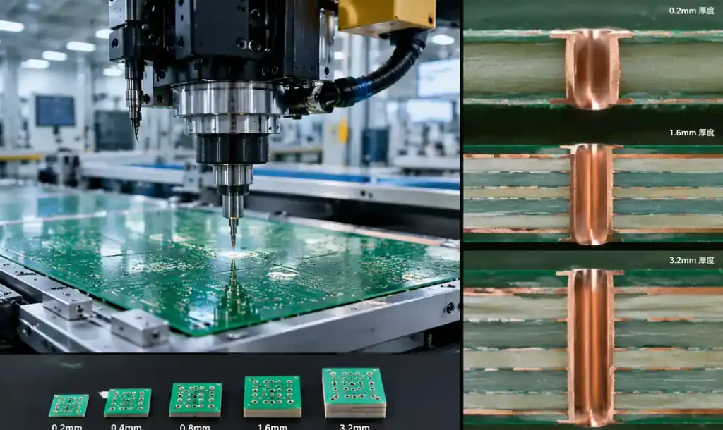
You should request stackup proposals from your manufacturer during design phase to verify feasibility. Andwin Circuits provides engineering support for custom thickness stackup design with up to 50 layers capability.
PCB Thickness Tolerances and Specifications
IPC-6012 defines thickness tolerances based on board construction and quality class. Standard tolerance is ±10% for Class 1/2 boards and ±0.13 mm for Class 3 boards. Tighter tolerances (±0.05 mm) are available for applications requiring precise connector fit or controlled impedance, but increase cost by 10-20% and may extend lead time. Most applications function reliably within standard IPC tolerances without premium specifications.
Design Best Practices for Thickness Selection
Start with standard 1.6 mm thickness during initial design unless specific constraints require alternatives. This minimizes cost, reduces lead time, and simplifies component selection. Evaluate mechanical stress, thermal requirements, and electrical performance to confirm suitability. Consider board support structures and component placement to maximize strength without increasing thickness. Consult PCB capability tables to understand manufacturer limitations for drill sizes and layer counts at various thicknesses.
FAQ
What is the most common PCB thickness?
The most common PCB thickness is 1.6 mm (0.062 inch), representing approximately 60% of all commercial PCB production worldwide. This thickness provides optimal mechanical strength, connector compatibility, and cost-effectiveness for most electronic applications from consumer devices to industrial equipment.
How much does custom PCB thickness cost compared to standard?
Custom PCB thickness adds 15-30% cost premium compared to standard 1.6 mm boards, with higher premiums for prototype and low-volume production. The cost difference includes custom material procurement, specialized tooling setup, and extended manufacturing lead time of 3-7 additional days depending on volume.
Can thin PCBs handle high-power applications?
Thin PCBs (0.8-1.0 mm) are generally unsuitable for high-power applications due to limited copper weight capacity, reduced heat dissipation, and mechanical strength concerns. Power electronics typically require 1.6-2.4 mm thickness to support heavy copper (3-6 oz), manage thermal loads, and provide structural stability for large components.
What thickness should I choose for impedance-controlled designs?
Standard 1.6 mm thickness is recommended for impedance-controlled designs because established stackup configurations reliably achieve 50-ohm and 100-ohm impedances with ±10% tolerance per IPC-2141. Custom thicknesses require detailed impedance calculation and stackup verification, potentially increasing design complexity and cost.
Does PCB thickness affect signal integrity?
PCB thickness indirectly affects signal integrity through dielectric layer spacing, which determines characteristic impedance and electromagnetic coupling between traces. Thicker boards provide more spacing between layers but require careful stackup design to maintain controlled impedance. Standard thicknesses offer proven signal integrity performance for high-speed digital and RF applications.
What is the thinnest PCB possible?
The thinnest commercially manufactured PCB is approximately 0.2 mm for specialized flexible circuits and ultra-compact devices. However, 0.6-0.8 mm represents the practical minimum for rigid PCBs with acceptable mechanical strength and manufacturing reliability. Thinner boards require specialized handling, support structures, and careful design consideration.
Conclusion
PCB thickness selection balances mechanical requirements, electrical performance, connector compatibility, and cost considerations. Standard 1.6 mm thickness provides optimal value for most electronic products with established manufacturing processes, reliable quality, and fast turnaround. Custom thickness is justified only when specific mechanical constraints, connector specifications, or specialized applications cannot be met with standard options.
If you need high-quality PCB manufacturing for your electronic devices, Andwin Circuits offers complete fabrication services with standard and custom thickness options up to 50 layers and fast delivery in 7 days. Our facility maintains ISO 9001, IATF 16949, and UL certifications for automotive, medical, telecommunications, and industrial applications worldwide. We provide engineering support for thickness selection, stackup design, and DFM optimization to ensure your products meet performance requirements while controlling costs.
Contact us today for custom PCB solutions, technical specifications, and competitive factory-direct pricing for your next project.