
PCB Soldermask: Color, Type, and Registration Requirements
When a PCB assembly fails at 0.3mm BGA pitch, the investigation often traces back to soldermask registration drift of just 75 microns. This isn’t theoretical—it’s a reality in high-density designs where soldermask performance directly impacts yield and reliability.
Soldermask serves as the primary insulation barrier between copper features, but its role extends beyond basic protection. The type you select, registration accuracy, and even color influence inspection efficiency, impedance control, and assembly outcomes. This guide synthesizes manufacturing experience with IPC standards to help you specify soldermask parameters that match your application’s requirements.
Understanding Soldermask Types and Chemistry
Modern PCB fabrication relies on two primary soldermask technologies, each with distinct process characteristics affecting registration accuracy and feature resolution.

Liquid Photoimageable (LPI) Soldermask
LPI soldermask dominates production volumes because it delivers repeatable registration at competitive cost. The liquid epoxy formulation gets screen-coated or curtain-coated onto copper surfaces, then UV-exposed through a phototool. Unexposed material washes away during development, leaving precise openings over pads.
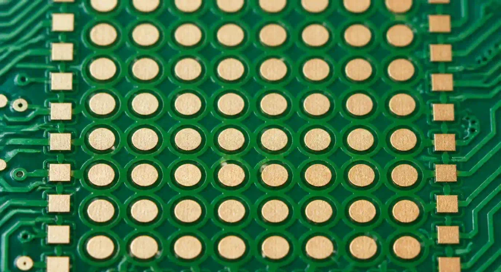
LPI typically achieves 0.8 to 1.2 mils (20-30 μm) thickness over copper. This controlled thickness matters for BGA and QFN packages where excessive mask dams between pads create bridging risks. Production data shows LPI maintains ±3 mil (±75 μm) registration tolerance—adequate for most 0.4mm pitch BGAs but marginal at 0.3mm.
LPISM for HDI Applications
High-density interconnect boards with microvias require LPISM formulations engineered for thin, uniform coatings. These masks cure to 0.4-0.6 mils (10-15 μm) thickness, reducing dam height between pads and improving laser via registration.

LPISM process control becomes critical for via-in-pad designs requiring mask-defined openings smaller than 4 mils. The thinner coating conforms better to surface topography but demands stricter exposure parameters to avoid curing failures or adhesion issues under thermal cycling.
| Parameter | LPI Soldermask | LPISM (HDI) |
|---|---|---|
| Typical Thickness | 0.8-1.2 mils (20-30 μm) | 0.4-0.6 mils (10-15 μm) |
| Registration Tolerance | ±3 mils (±75 μm) | ±2 mils (±50 μm) |
| Minimum Opening | 4 mils (0.1 mm) | 3 mils (75 μm) |
| Suitable Pitch | ≥0.4 mm BGA | ≥0.3 mm BGA, microvia |
| Cost Multiplier | 1.0x baseline | 1.3-1.6x |
Soldermask Color Selection for Functional Requirements
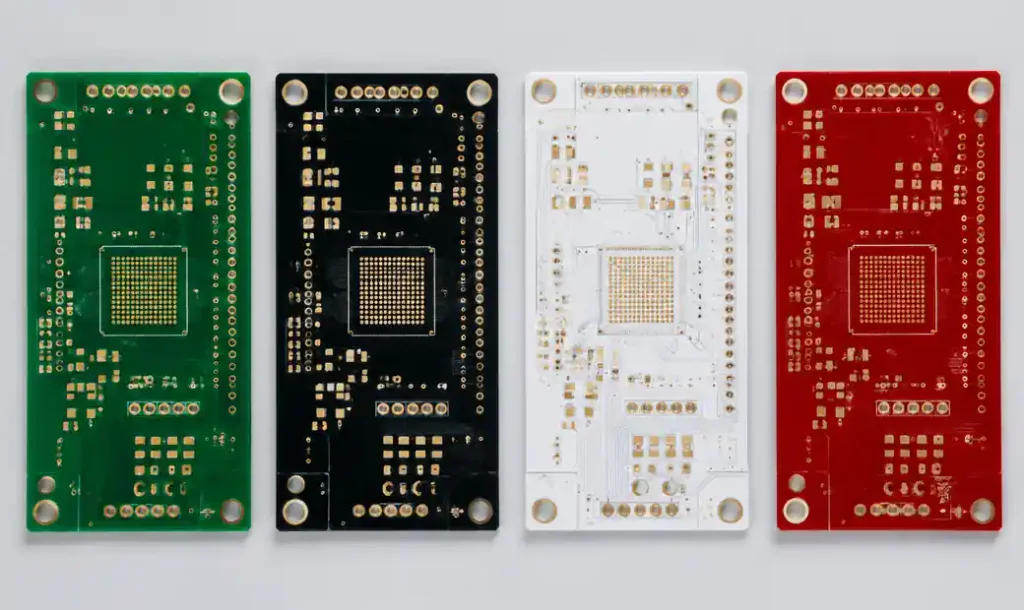
Green soldermask earned ubiquity through manufacturing economics—early epoxy formulations naturally cured to green, and AOI systems optimized algorithms around that wavelength contrast. But color choice affects more than aesthetics.
Inspection and Contrast Considerations
Black soldermask conceals trace routing on consumer electronics but reduces AOI defect detection rates by 15-20% compared to green because copper trace contrast drops significantly. White masks maximize light reflectivity for LED boards but create glare during manual inspection under magnification.
Red masks deliver highest contrast for visual inspection of solder joint quality. We specify red for prototypes and first-article builds where operators perform detailed inspection, then switch to green for production once process stability is confirmed.
Thermal and Electrical Performance
Soldermask color influences surface temperature by 3-5°C in high-power applications due to varying thermal emissivity. Black absorbs more radiant heat. White reflects heat but shows contamination more readily.
Pigment loading for different colors affects dielectric properties slightly—darker colors may introduce fractionally higher dissipation factors, though impact remains negligible below 10 GHz. For mmWave designs above 24 GHz, specify low-Dk soldermask formulations regardless of color.
| Color | Best Application | Inspection Contrast | Typical Cost |
|---|---|---|---|
| Green | General purpose, high volume | Excellent (baseline) | Standard |
| Black | Consumer electronics, aesthetics | Poor (-20% defect detection) | +10-15% |
| White | LED boards, high reflectivity | Good (glare under magnification) | +15-20% |
| Red | Prototypes, quality inspection | Excellent (best visual contrast) | +10-15% |
| Blue | Differentiation, medical devices | Good | +15-20% |
Registration Accuracy and Pad Opening Design
Registration tolerance defines how precisely soldermask openings align to underlying pad geometry. This alignment directly affects solder paste printing, component placement, and occurrence of bridges or insufficient filleting.
IPC-6012 Class Requirements
IPC-6012 establishes three performance classes. Class 2 (general industrial) permits ±4 mil misregistration between mask opening and pad edge. Class 3 (high reliability) tightens this to ±3 mil for safety or mission-critical applications.
Class 3A has emerged in aerospace and medical device specifications requiring ±2 mil registration. Achieving this demands process controls beyond typical commercial fabrication—substrate material with CTE below 50 ppm/°C, registration fiducials on every panel, and dimensional verification at multiple process stages.
Solder Mask Defined vs. Non-Solder Mask Defined Pads
The decision between SMD and NSMD pads affects reliability more than any other soldermask specification for fine-pitch BGAs.
NSMD pads expose copper slightly larger than the mask opening, creating positive offset of typically 2-4 mils per side. This design tolerates registration variation because the solder ball contacts copper even when mask registration drifts. NSMD is the IPC-7095 recommended approach for BGA pitch ≤0.5mm because it improves solder joint fatigue life by eliminating stress concentration at the mask-to-copper interface.
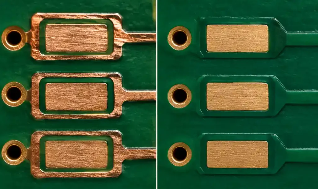
SMD pads have mask openings smaller than copper pad, which defines the solderable area. This can increase routing density but creates brittle joints where the ball adheres to both copper and mask sidewall. Thermal cycling induces shear stress at that interface, and joints crack after fewer cycles than equivalent NSMD designs.
Practical Opening Dimensioning
For NSMD designs, subtract 3-4 mils per side from pad diameter to create positive clearance accommodating registration variation. A 16 mil NSMD pad would specify a 10 mil mask opening (16 – 2×3 mil).
Minimum web width between adjacent mask openings should not fall below 4 mils for standard LPI or 3 mils for LPISM. Narrower webs tear during development or delaminate under reflow thermal stress.
Soldermask Impact on Impedance Control
Controlled impedance transmission lines require soldermask presence in your field solver model because the mask’s dielectric constant alters the effective Er. Ignoring this introduces 3-8% impedance error depending on trace geometry and mask thickness.

Dielectric Constant Variation
Standard LPI soldermask exhibits Dk of 3.3-3.8 at 1 MHz. Low-Dk soldermask formulations target Dk ≤3.0 for high-speed digital and RF applications where impedance tolerance affects bit error rates or return loss. These materials cost 40-60% more than standard masks.
Request soldermask dielectric test data from your fabricator when designing impedance-critical boards. Generic datasheet values reflect typical performance but your specific board may receive material from a different batch with measurably different properties.
Coplanar Waveguide and Mask Coverage
Coplanar waveguide transmission lines assume soldermask covers ground features uniformly. If you specify mask pullback on grounds for thermal relief or test point access, exposed copper locally reduces impedance by increasing capacitance to the reference plane.
Model these soldermask openings in your field solver or widen the trace temporarily where mask must be removed to compensate for capacitance increase.
FAQ
What soldermask registration tolerance do I need for 0.4mm pitch BGA?
IPC-7095 recommends NSMD pad design with ±3 mil (±75 μm) registration tolerance for 0.4mm BGA pitch. This provides adequate process margin when using standard LPI soldermask on dimensionally stable substrate materials. Tighter tolerance becomes necessary at 0.3mm pitch.
Does soldermask color affect electrical performance?
Soldermask color has negligible impact on electrical performance for frequencies below 10 GHz. Pigment loading creates minor Dk variations (typically <0.2), but this falls within normal batch-to-batch material variation. For mmWave applications above 24 GHz, specify low-Dk soldermask formulations and verify dielectric properties through testing regardless of color.
When should I use SMD versus NSMD pads?
Use NSMD (non-solder mask defined) for BGA pitch ≤0.5mm and all high-reliability applications. NSMD improves solder joint fatigue life by eliminating stress concentration at the mask edge. SMD pads may suit larger pitch components where routing density between pads is constrained, but accept reduced thermal cycling performance.
What minimum soldermask web width is manufacturable?
Standard LPI soldermask supports 4 mil (0.1mm) minimum web width between openings. LPISM formulations can achieve 3 mil webs with tighter process control. Narrower webs risk tearing during development or delamination under thermal stress.
How does soldermask thickness affect BGA assembly?
Excessive soldermask thickness creates tall dams between BGA pads that trap solder paste and prevent proper ball collapse during reflow. Standard LPI at 0.8-1.2 mils works for ≥0.4mm pitch. Finer pitch BGAs require LPISM at 0.4-0.6 mils to reduce dam height and improve paste release.
Can I mix soldermask colors on one board?
Dual-color soldermask requires two separate mask coating and imaging processes, which doubles mask cost and introduces registration risk between colors. This approach occasionally appears in high-end consumer products for aesthetic differentiation but is impractical for functional requirements.
Conclusion
Soldermask specification directly determines whether your PCB design transitions from prototype to reliable production without yield losses or field failures. Registration tolerance, opening design methodology, and material selection must align with your component pitch and reliability requirements—±3 mil registration with NSMD pads works for most industrial applications at 0.4mm BGA pitch, while tighter tolerance and LPISM become mandatory below 0.3mm.
Color selection balances inspection efficiency against aesthetic requirements, with green remaining the practical choice for AOI throughput and cost control. Request soldermask dielectric data when designing impedance-critical boards, and verify registration capability through first-article inspection before committing to production volumes. Work with your PCB fabricator early in the design phase to verify registration capability, review pad geometry, and confirm mask opening dimensions. For projects requiring Class 3 reliability or fine-pitch BGAs, consider Andwin Circuits’ soldermask process qualification and AOI inspection capabilities.