
Blind and Buried Via Design: Cost vs Benefit Analysis
Blind and buried vias add $28-$85 per board for Type I HDI and $150-$350+ for Type III at prototype volumes—a 300-600% premium over through-hole vias. Engineers designing smartphones, wearables, and compact IoT devices face a choice: pay for density or accept larger boards. This analysis shows when routing benefits justify the investment and when standard vias suffice.
Understanding Blind and Buried Via Structures
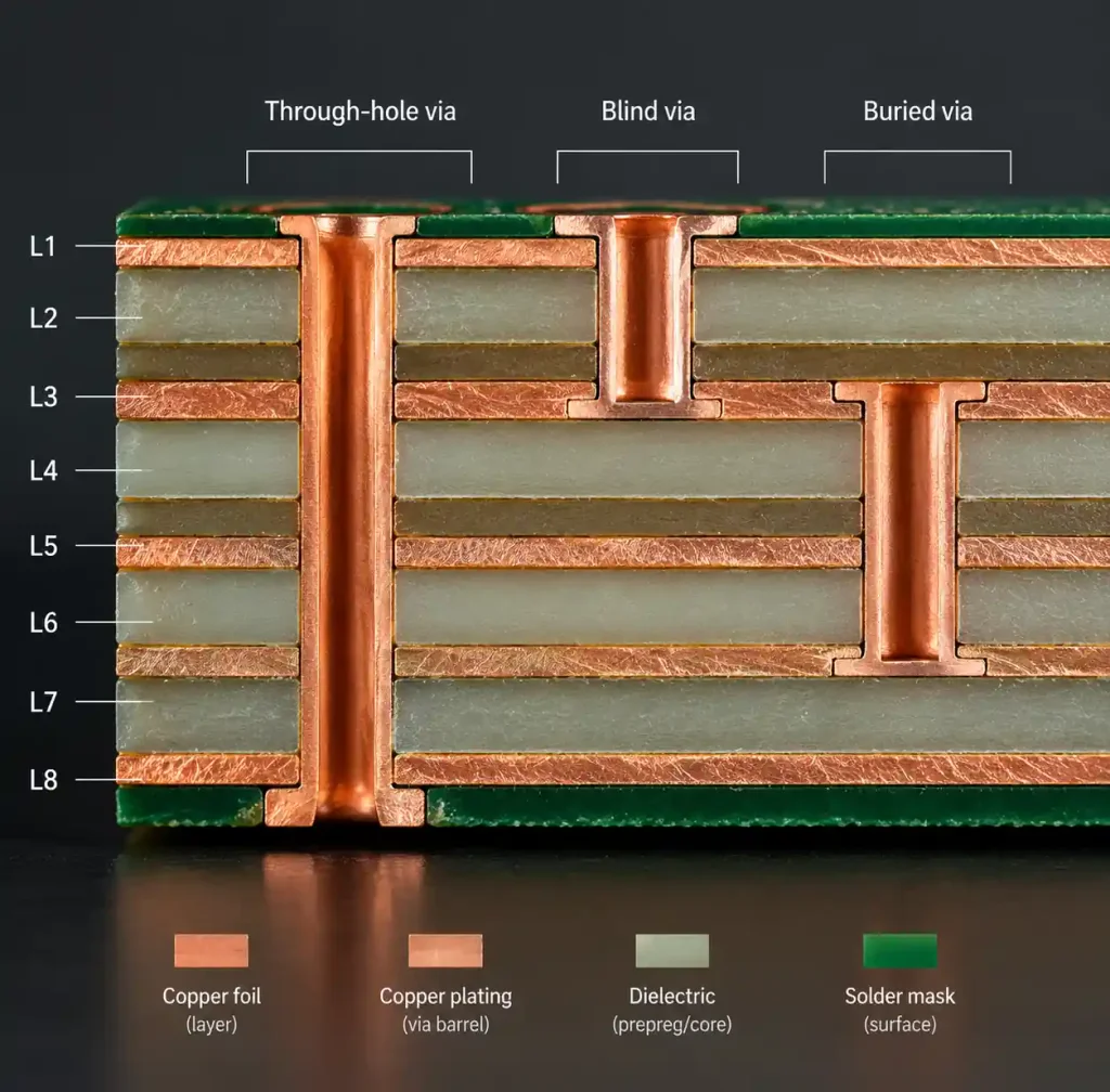
Through-hole vias penetrate the entire PCB thickness, consuming routing space on every layer. An 8-layer board with 50 through-hole vias blocks 400 via locations (50 × 8 layers), limiting trace routing.
Blind vias connect an outer layer to inner layers without reaching the opposite surface. L1 to L3 in an 8-layer stackup leaves L4-L8 free for routing. Buried vias connect only internal layers (L3 to L6), invisible from both surfaces.
Microvias are blind vias with 0.15mm or smaller diameter, created through laser drilling. They span one or two layers maximum, enabling HDI PCB build-up with 1+N+1 or 2+N+2 configurations per IPC-2226.
Manufacturing requires sequential lamination—building the board in stages. Type I HDI (1+N+1) uses one build-up layer per surface. Type II (2+N+2) stacks microvias across two build-up layers. Type III incorporates buried vias within the core, demanding three or more lamination cycles.
Cost Structure: Process Complexity Drives Pricing
Blind and buried via costs stem from process complexity, not materials. Sequential lamination, laser drilling, and via filling add steps that standard boards avoid.
Laser Drilling: Mechanical drills cost $15-$50 panel setup plus $0.002-$0.008 per hole. CO2 or UV lasers cost $80-$250 per panel plus $0.008-$0.025 per via—4-5x higher for 200-via panels.
Sequential Lamination: Each build-up layer needs copper application, imaging, etching, and oxide treatment. Type I HDI adds 2-3 days and $12-$25 per board. Type III adds $45-$85 and 5-7 days.
Via Filling: Resin plugging for via in pad costs $8-$15 per board. Copper-filled and planarized vias add $18-$35. Through-holes use soldermask tenting at no extra cost.
| Via Type | Drilling Method | Setup Cost/Panel | Per-Via Cost | Lamination Cycles | Cost Premium/Board (Prototype) |
|---|---|---|---|---|---|
| Through-Hole | Mechanical | $15-$50 | $0.002-$0.008 | 1 cycle | Baseline |
| Blind Microvia (Type I) | CO2 laser | $80-$250 | $0.008-$0.025 | 2 cycles | +$28-$85 |
| Stacked Microvia (Type II) | UV laser | $100-$280 | $0.012-$0.035 | 3 cycles | +$72-$165 |
| Buried Via (Type III) | Mech + laser | $150-$350 | $0.015-$0.045 | 3-4 cycles | +$150-$350+ |
Volume production reduces per-board costs. A 10,000-unit run drops Type I HDI premiums to $8-$18 versus prototypes. NRE for tooling and testing adds $800-$2,500 for HDI designs requiring impedance control verification.

Routing Density Benefits: Quantifiable Space Savings

Blind and buried vias unlock routing channels that through-holes block. An 8-layer board with L1-L3 blind vias frees 62.5% of via space (5 of 8 layers) versus through-holes consuming all layers.
Component Density: A 0.5mm pitch BGA with 225 balls needs 180-200 escape vias. Through-hole vias require 0.8mm pads, blocking adjacent channels. Microvias use 0.5mm pads, allowing 60% tighter spacing and fitting between BGA pads.
Layer Reduction: Smartphones achieve 12-14 layer complexity in 8-10 layers through blind vias. Each eliminated layer pair saves $8-$15 per board—offsetting HDI premiums above 5,000-8,000 units.
Signal Integrity: Through-hole vias in 1.6mm boards create 1.6mm stubs generating reflections above 5-8 GHz. Blind vias terminate at target layers with 0.2-0.4mm stubs—75-85% reduction improving USB, PCIe, and HDMI performance.
Area savings reach 15-30% depending on density. A 40×60mm design with 400-pin BGA shrinks to 35×50mm with Type I HDI—27% reduction worth $3-$8 per board at volume.
HDI Stackup Integration: Build-Up Structures
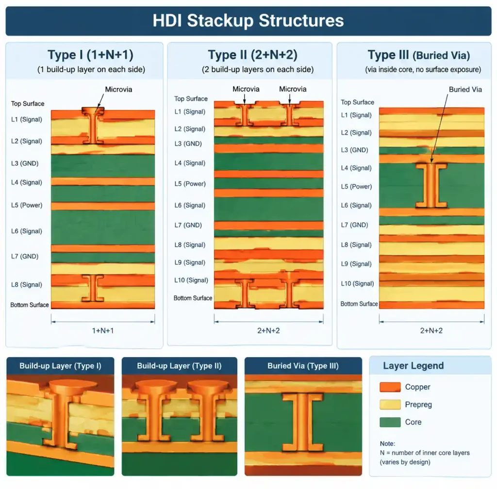
HDI terminology follows IPC-2226 where “N” represents core layers. Type I (1+N+1) adds one microvia layer per surface. Type II (2+N+2) stacks two layers per side. Type III adds buried vias within the core.
Type I (1+N+1): L1 microvias reach L2; L8 microvias reach L7 in 8-layer boards. Suits moderate-density designs requiring 30-40% more routing than standard boards. Cost: $28-$85 per board at prototype volumes.
Type II (2+N+2): Stacked (L1→L2→L3) or staggered microvias increase routing 60-80% over through-holes. Used in smartphones and wireless modules for 0.4-0.5mm pitch BGAs. Cost: $72-$165 per board.
Type III: Buries high-speed pairs or power distribution on internal layers. Automotive radar, 5G, and AI accelerators use buried vias for controlled impedance with minimal discontinuities. Cost: $150-$350+ per board.
Not all PCB manufacturers offer Type III capability. Lead times vary 7-21 days depending on complexity. IPC-2226 provides design guidelines, IPC-6016 covers qualification.
Decision Framework: When Blind and Buried Vias Justify Cost
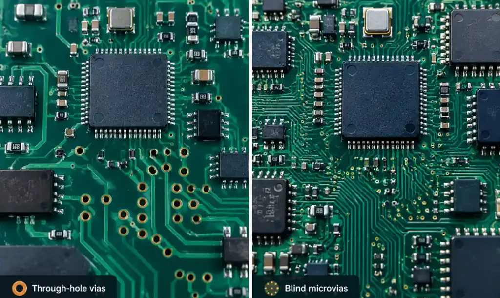
Three factors determine HDI via justification: routing density, component pitch, and volume. Cost-benefit analysis should account for board-level savings (area, layers) and manufacturing trade-offs (lead time, yield, rework difficulty).
Routing Density: Designs with >60% trace utilization hit congestion forcing additional layers or larger dimensions. Through-holes create 0.8-1.2mm keepout zones versus 0.5-0.6mm for blind vias—40-50% penalty. If adding two layers costs $16-$30 per board, Type I HDI at +$28-$85 makes sense when layer reduction or volume exceeds 3,000-5,000 units.
Component Pitch: BGAs below 0.65mm pitch and QFNs with 0.4mm pad spacing cannot escape through-holes without HDI. Physical geometry forces the choice. Standard electronics with 0.8mm+ pitch use through-holes until density limits emerge.
Production Volume: Prototypes (10-100 boards) absorb full NRE and setup costs. At 5,000+ units, panel utilization amortizes premiums. Break-even for 8-layer Type I HDI versus 10-layer through-hole: HDI costs $85 prototype/$18 at 10K; standard costs $55 prototype/$22 at 10K. Break-even: 6,500-8,000 units.
| Design Requirement | Through-Hole Via | Blind Via (Type I) | Buried Via (Type III) | Recommendation |
|---|---|---|---|---|
| 0.8mm+ BGA, <50% routing density | ✓ Adequate | Overkill | Unnecessary | Use through-hole |
| 0.5-0.65mm BGA, 60-75% density | Marginal | ✓ Optimal | Overkill | Type I HDI justified |
| <0.5mm pitch, >75% density | Impossible | Insufficient | ✓ Required | Type II/III HDI required |
| High-speed SerDes, DDR5, PCIe Gen 5 | Signal integrity issues | ✓ Improved performance | ✓ Best SI | HDI reduces stub reflections |
| Volume <1,000 units | ✓ Cost-effective | Use if density forces | Use if no alternative | Minimize HDI complexity |
| Volume >10,000 units | Larger boards | ✓ Cost-neutral with savings | ✓ Economical if needed | Evaluate total cost of ownership |
Design Considerations and Reliability
HDI vias introduce manufacturing variables affecting yield and reliability. Design rules must account for laser drilling tolerances, registration accuracy, and thermal stress.
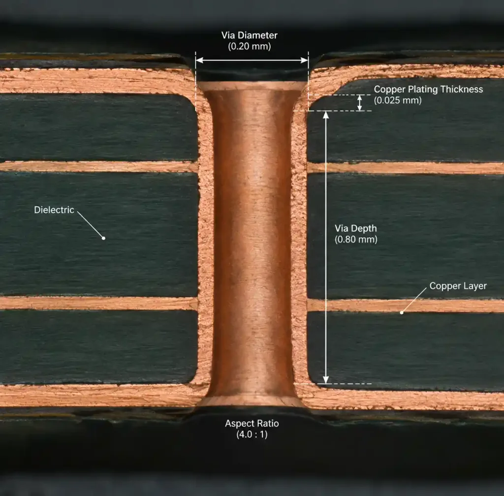
Aspect Ratio Limits: Through-holes maintain 10:1 aspect ratio (thickness to diameter). Blind vias should not exceed 0.8:1 for mechanical or 0.6:1 for laser drilling. A 0.2mm blind via spans 0.12-0.16mm depth reliably—roughly 1-2 layers.
Registration Accuracy: Sequential lamination accumulates ±0.075mm tolerance per layer, compounding to ±0.15mm for Type II. Stacked microvias need 0.05mm capture pad margins. Specify ±0.05mm for Type III and verify manufacturer capability.
Thermal Cycling: IPC-6016 Class 3 requires 500 cycles (-55°C to +125°C) for automotive/aerospace. Buried vias experience higher CTE mismatch stress than through-holes. Specify high-Tg materials (170°C+) and 2oz+ copper for reliability-critical designs.
Via Filling Quality: Incomplete resin filling traps flux and moisture, failing during thermal shock. IPC-4761 Type VII (fully filled and planarized) ensures reliable BGA assembly but adds $15-$25 per panel for X-ray inspection.
FAQ
How much do blind and buried vias increase PCB cost?
Type I HDI adds $28-$85 per board at prototype quantities (10-50 units) and $8-$18 at 10,000+ volume. Type II costs $72-$165 for prototypes, $18-$35 at volume. Type III runs $150-$350+ for prototypes due to 3-4 lamination cycles and extended lead times. Always request quotes with actual Gerber files.
Can blind vias reduce total PCB cost through layer count reduction?
Yes, at volumes above 5,000-8,000 units. An 8-layer HDI board may replace a 10-layer through-hole design. Eliminating two layers saves $16-$30 per board, offsetting the $8-$18 HDI premium at volume. Run cost models with your manufacturer to identify break-even points.
What minimum feature sizes do manufacturers support?
Most manufacturers handle 0.15mm microvias (6 mil) with 0.35mm pads for Type I HDI. Advanced manufacturers achieve 0.10mm (4 mil) holes with 0.25mm pads. Buried vias typically use 0.20-0.30mm mechanical drilling. Laser tolerances are ±0.025mm versus ±0.05mm for mechanical drilling.
Do blind and buried vias affect signal integrity?
Blind vias improve high-speed signal integrity by eliminating via stubs. Through-hole vias in 1.6mm boards create 1.6mm stubs generating reflections above 5-8 GHz. Blind vias terminate at target layers with 0.2-0.4mm stubs—75-85% reduction. This improves USB 3.2, PCIe Gen 4-5, HDMI 2.1, and 10+ Gbps SerDes eye diagrams.
What are the main reliability concerns?
Incomplete plating in high aspect ratio blind vias (>0.8:1) causes failures after thermal cycling. Registration errors between build-up layers misalign stacked microvias. Resin-filled vias may contain voids trapping moisture. Specify IPC-6016 Class 3 testing for medical, automotive, and aerospace applications requiring 15-25 year lifespans. Use high-Tg materials (170-180°C) and heavy copper (2-3 oz).
Conclusion
Blind and buried vias deliver 30-60% more routing density and 15-30% board area reduction but cost 3-6x more than through-holes at prototype volumes. The decision hinges on whether component pitch forces HDI (<0.65mm BGA), whether layer reduction offsets premiums at volume (break-even at 5,000-8,000 units), and whether signal integrity demands shorter stubs above 10 GHz.
Evaluate Type I HDI when routing congestion exceeds 60-70% or fine-pitch BGAs appear. Prototype 10-50 boards to validate design rules and yields before volume production. Work with manufacturers offering IPC-6016 certification, <0.05mm registration, and microsection analysis to avoid redesigns. For high-volume products, model total cost including area savings and layer reduction—HDI justifies its premium when density gains enable miniaturization that through-holes cannot achieve.