
PCB Design for EMC: Layout Techniques to Pass Radiated Emissions Testing
Radiated emissions failures account for roughly 60% of all first-time EMC test failures in my experience working with over 200 PCB designs. The frustrating part? Most of these failures stem from layout decisions made weeks before anyone thinks about compliance testing. After spending countless hours in semi-anechoic chambers diagnosing failures at 87 MHz, 230 MHz, and other problematic frequencies, I’ve learned that passing radiated emissions testing isn’t about luck—it’s about understanding how your PCB actually radiates and controlling it at the design stage. At Andwin Circuits, we’ve refined these techniques through extensive testing and real-world manufacturing experience.
Why Layout Matters More Than You Think
Every trace on your PCB is a potential antenna. When high-frequency current flows through a trace and returns through a plane or another conductor, the loop area formed between them becomes a radiating structure. The radiated field strength increases proportionally with frequency, current, and loop area. This is why a seemingly innocent 50 mm² loop carrying a 100 MHz clock can fail FCC Class B limits by 10-15 dB, while a well-designed 5 mm² loop passes with margin. Understanding PCB electromagnetic compatibility (EMC) design principles is essential for creating boards that pass testing consistently.
The problem intensifies with modern designs. As clock speeds push past 500 MHz and edge rates drop below 1 ns, even a 20 mm trace becomes electrically significant. The seventh harmonic of a 200 MHz clock sits at 1.4 GHz—right in the middle of cellular bands where emission limits are strictest.
Critical Layout Techniques That Actually Work
Stack-Up Configuration: Your First Line of Defense
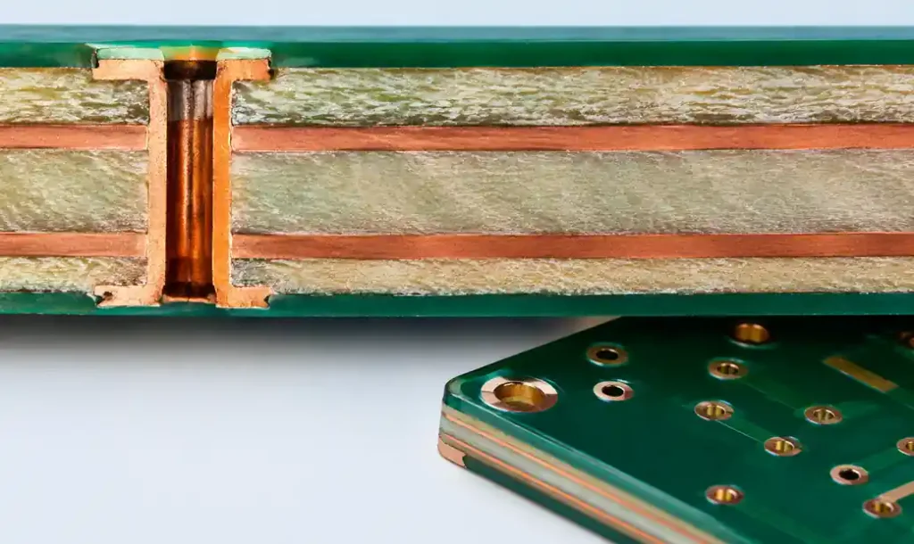
I consistently recommend 4-layer PCB boards with a dedicated ground plane for any design with clocks above 25 MHz. The stack-up sequence matters tremendously. Place your high-speed signals on the layer immediately adjacent to the ground plane—this minimizes loop area by keeping the return path close.
| Stack-Up Type | Typical Loop Area | First-Time Pass Rate | Cost Premium |
|---|---|---|---|
| 2-layer | 500-2000 mm² | 35-45% | Baseline |
| 4-layer (optimized) | 10-50 mm² | 75-85% | +25-35% |
| 6-layer (controlled) | <5 mm² | 90-95% | +50-70% |
The cost difference between 2-layer and 4-layer boards has narrowed to roughly 30% for most mid-volume orders. When you factor in the $15,000-$25,000 cost of EMC test chamber time plus engineering rework, the 4-layer investment pays for itself immediately.
Component Placement: Where Problems Start
I place all high-frequency components (crystals, oscillators, processors) as close to the board center as possible—never near edges or corners where radiation couples most efficiently to enclosure seams. Clock generators sit within 15 mm of their loads when feasible. This isn’t just good practice; it’s the difference between a clean spectrum and a 20 dB spike at your clock fundamental. Thoughtful PCB component placement directly impacts your emission test results.
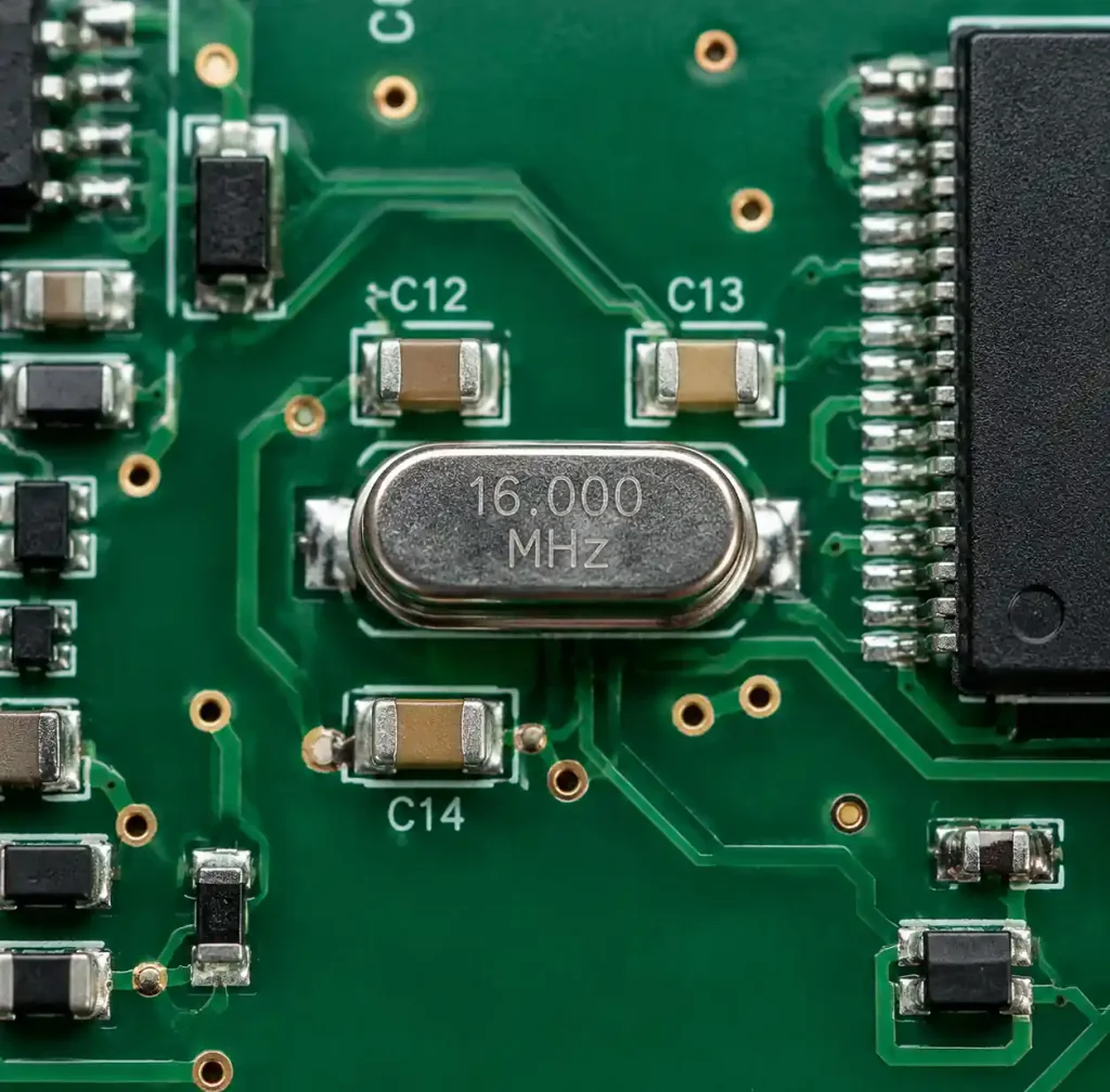
Keep crystals and their loading capacitors within a 10 mm radius. The loop formed by crystal-capacitor-IC must be minuscule. I’ve seen designs fail at 27 MHz simply because someone placed loading caps 40 mm away from the crystal, creating a beautiful dipole antenna.
Routing Strategies for High-Speed Signals
Route all clock traces on the layer directly above the ground plane. Never switch layers mid-trace unless absolutely necessary, and when you must, place a ground via within 2 mm of the signal via. This maintains return path continuity and prevents the formation of large radiation loops.
For differential pairs like USB, HDMI, or LVDS, maintain symmetry ruthlessly. Length mismatch should stay under 5 mils for USB 2.0 and 0.5 mm for most other differential pairs. More importantly, keep the pair routed together—gaps longer than 3× the trace width break the field cancellation that makes differential signaling work. Proper PCB signal integrity considerations are critical for maintaining clean emissions profiles.
| Signal Type | Max Loop Area | Routing Layer | Via Strategy | Critical Frequency |
|---|---|---|---|---|
| Clock (>100 MHz) | <25 mm² | Adjacent to GND | GND via at transitions | 7th harmonic |
| Differential USB 2.0 | <15 mm² | Adjacent to GND | Paired signal+GND vias | 480 MHz + harmonics |
| SPI/I2C (<20 MHz) | <200 mm² | Any layer | Standard | 3rd harmonic usually safe |
| Ethernet (GbE) | <10 mm² | Stripline preferred | Balanced pairs | 625 MHz + harmonics |
Ground Plane Integrity: The Foundation Everything Builds On
A solid, uninterrupted ground plane is non-negotiable. Every slot or split in the ground plane forces return currents to detour around it, increasing loop area and radiation. I’ve measured 15-20 dB improvements simply by removing unnecessary ground plane cuts. Proper grounding strategies form the backbone of effective EMC design.
When you must route signals through a split (power island boundaries, etc.), place the split perpendicular to signal flow and bridge it with multiple 0.01 µF decoupling capacitors spaced every 20-30 mm. These capacitors provide a high-frequency return path across the split.
Decoupling: More Than Just Capacitors on Power Pins
Inadequate decoupling causes two problems: power rail noise that directly radiates from power traces, and voltage fluctuations that modulate signal transitions and create spectral spreading. Both are emissions disasters.
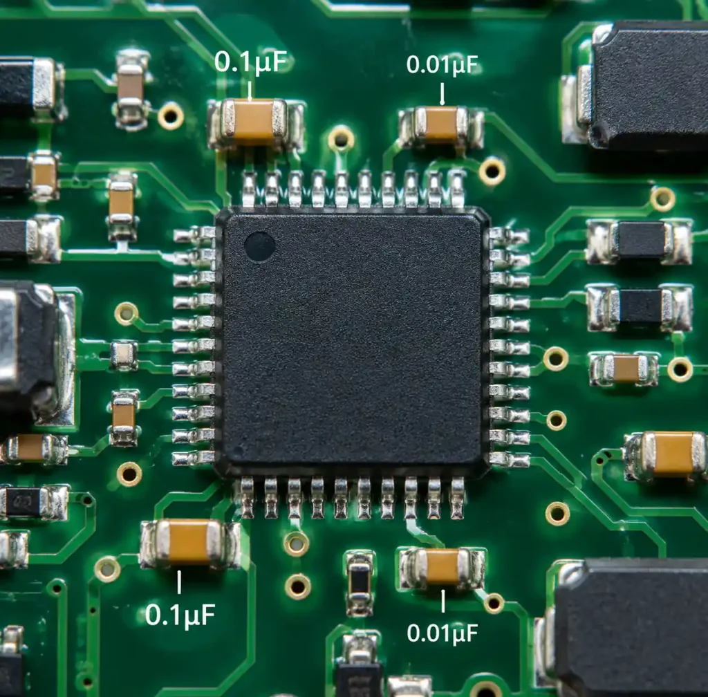
Place one 0.1 µF ceramic capacitor within 5 mm of every IC power pin. For high-speed processors, add 0.01 µF caps within 2 mm of the pin—closer than your 0.1 µF caps. The via path from power pin to capacitor to ground must be as short as physically possible. I target <10 mm total trace length for this loop.
Add bulk capacitance (10-100 µF) near power entry points and at high-current ICs. Tantalum or polymer aluminum capacitors work well here. The goal is supporting transient current demands locally, preventing high-frequency noise from propagating back to power supplies where it can radiate from cables.
Managing Common-Mode Currents
Common-mode currents—currents flowing in the same direction on both conductors of a pair—are responsible for most radiated emissions from cables. They arise when signal return currents don’t flow exclusively through intended return paths but leak onto chassis, cables, or other unintended structures.
Ferrite Beads and Common-Mode Chokes
Place ferrite beads on all cables leaving the PCB—USB, Ethernet, power cables. The ferrite bead impedance should peak at your problem frequencies. For typical digital designs, I specify beads with peak impedance at 100-300 MHz. Don’t forget ground connections; a ferrite bead on a power cable without ground filtering is only half-effective.
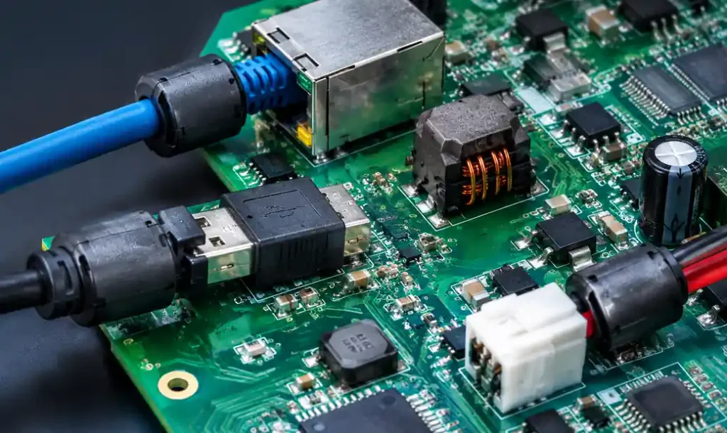
Common-mode chokes work exceptionally well on differential pairs. A single CM choke on an Ethernet pair can provide 20-30 dB suppression above 100 MHz. The differential signal passes through unaffected while common-mode noise sees high impedance.
Edge Rate Control: The Overlooked Solution
Faster edge rates generate stronger high-frequency harmonics. A 2 ns edge rate produces significant energy up to 500 MHz (approximately 0.35 / rise time). Slowing edges to 5 ns cuts harmonic content above 200 MHz dramatically—often by 15-20 dB.
Most modern drivers offer programmable slew rate control. Use it. If your signal timing budget allows 3 ns edges, don’t use 1 ns edges just because they’re available. I routinely specify moderate-speed buffers for non-critical signals. A 74LVC buffer with 5 ns edges is quieter than a 74AVC buffer with 1.5 ns edges, and for most control signals, you’ll never notice the speed difference.
Verification Before Manufacturing
I always run basic loop area calculations before releasing a design. Identify your three highest-frequency signals, measure their loop areas using your layout tool, and plug numbers into the radiated field equation. If calculated field strength approaches limits, fix the layout before fabrication.
Real-World Test Failures and Fixes
Case Study: 230 MHz Clock Harmonic
We had a design fail at 232 MHz—exactly the third harmonic of the 77.33 MHz pixel clock. Investigation revealed the clock trace ran 85 mm across the board on the top layer with ground return through vias to a bottom-layer plane. Moving the trace to layer 2 (adjacent to ground) and shortening it to 45 mm brought emissions down by 18 dB—well below limits.
Case Study: Power Trace Radiation
A client’s product failed radiated emissions testing at multiple frequencies between 150-400 MHz. The spectrum showed broadband noise rather than discrete harmonics, suggesting power distribution issues. We found the 3.3V power trace running the board perimeter, forming a massive loop. Replacing it with a power plane and adding localized decoupling dropped emissions 22 dB across the problematic range.
When Layout Alone Isn’t Enough
Sometimes even perfect layout can’t fully suppress emissions. In these cases, you need additional measures:
Shielding: Small metal cans over high-frequency sections (oscillators, RF sections) provide 20-40 dB additional suppression. Ensure multi-point grounding of shield cans—single-point grounding is ineffective above 100 MHz.
Spread-Spectrum Clocking: Spread-spectrum clock generators modulate the clock frequency slightly (typically ±0.5-2%), spreading harmonic energy across a bandwidth rather than concentrating it at discrete frequencies. This can reduce peak emissions by 10-15 dB, often just enough to pass. Trade-off is slightly increased jitter.
Filtered Connectors: Connectors with integrated capacitive or LC filtering suppress common-mode currents before they reach cables. Particularly effective for power and low-speed I/O.
FAQ
How do I know if my PCB design will pass radiated emissions testing before building it?
While you can’t guarantee compliance without testing, you can predict likely performance using loop area calculations for your highest-frequency signals. Calculate the loop area for each high-speed signal (clock, data buses), multiply by current and frequency squared, and compare to known problematic thresholds. Loops under 25 mm² for signals above 100 MHz typically pass. Also review component placement—high-frequency sources near board edges are red flags. Pre-compliance testing with near-field probes during prototyping can identify issues early.
What’s the most common radiated emissions failure you see?
Clock signal harmonics failing at the third, fifth, or seventh harmonic are by far the most common. This typically stems from excessive loop area caused by poor stack-up choices or signal routing on outer layers far from ground planes. The second most common issue is common-mode radiation from cables due to inadequate filtering or ground plane discontinuities near connectors.
Is a 2-layer board adequate for designs with high-speed signals?
For clock speeds under 25 MHz and careful layout, 2-layer boards can pass, but margins are thin. Above 50 MHz, 2-layer boards become increasingly difficult. I’ve seen 2-layer designs with 100+ MHz clocks pass, but they required extreme layout discipline, additional filtering, shielding, and usually multiple test iterations. The risk-adjusted economics strongly favor 4-layer boards for anything above 25 MHz.
How close should decoupling capacitors be to IC power pins?
For 0.1 µF bypass capacitors, target <5 mm from the capacitor body to the power pin. For 0.01 µF caps used with very high-speed parts, aim for <2 mm. What matters more than physical distance is loop area—measure the total trace length from power pin to capacitor to ground and back to IC ground pin. Keep this entire loop under 10 mm for best results.
Can I use spread-spectrum clocking to fix emissions problems?
Spread-spectrum clocking is a useful tool but not a magic fix. It typically provides 8-15 dB reduction in peak emissions at clock harmonics by spreading energy across a broader frequency range. This often converts a marginal failure into a pass. However, it doesn’t address common-mode emissions from cables or reduce total radiated power—just distributes it differently. Use it as a supplement to good layout, not a replacement.
What test equipment do I need for pre-compliance testing?
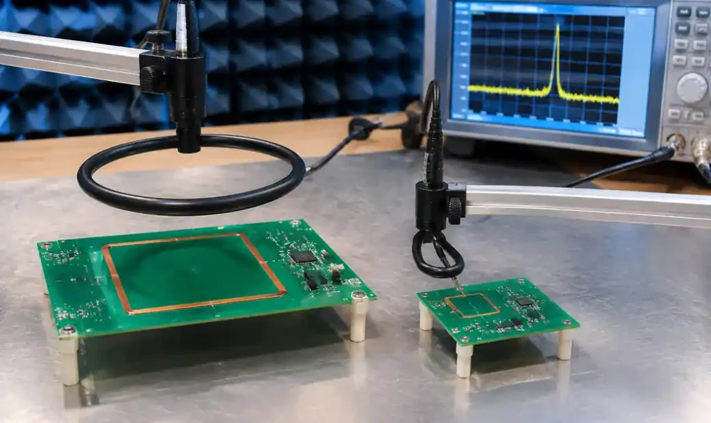
At minimum, a near-field probe set and spectrum analyzer let you identify problematic areas on your PCB before formal testing. Quality near-field probes cost $500-2000, and a basic spectrum analyzer capable of 3 GHz runs $3000-10,000. This investment pays for itself by catching issues during development rather than during $15,000 formal compliance tests. Many engineering labs offer probe set rentals if capital budget is constrained.
Conclusion
Passing radiated emissions testing demands more than following generic design rules—it requires understanding the physics of how PCBs radiate and systematically minimizing radiation paths. Every layout decision from PCB stack-up configuration through final routing either helps or hurts your emissions profile.
Focus on these core principles: minimize loop areas by placing signals adjacent to solid reference planes, maintain ground plane continuity ruthlessly, use adequate decoupling placed as close as physically possible to power pins, control edge rates to the slowest acceptable values, and keep high-frequency components away from board edges and openings. For designs above 100 MHz, 4-layer construction with proper stack-up isn’t optional—it’s foundational.
I’ve found that designs following these practices pass formal EMC testing on the first attempt 80-85% of the time, compared to industry averages around 50%. The remaining failures typically require minor tuning—adding a ferrite bead, adjusting a trace route, or implementing spread-spectrum clocking—rather than wholesale redesigns. When you understand how your board radiates, you design it not to.