
PCB Layout for DC-DC Converters: Buck, Boost, and Buck-Boost Design Strategies
Designing PCBs for DC-DC converters requires understanding that switching noise, thermal performance, and efficiency are all determined at the layout stage. After years of optimizing power converter PCBs for demanding applications, I’ve found that most performance issues trace back to three critical layout decisions made in the first hour of board design.
Understanding DC-DC Converter Topologies
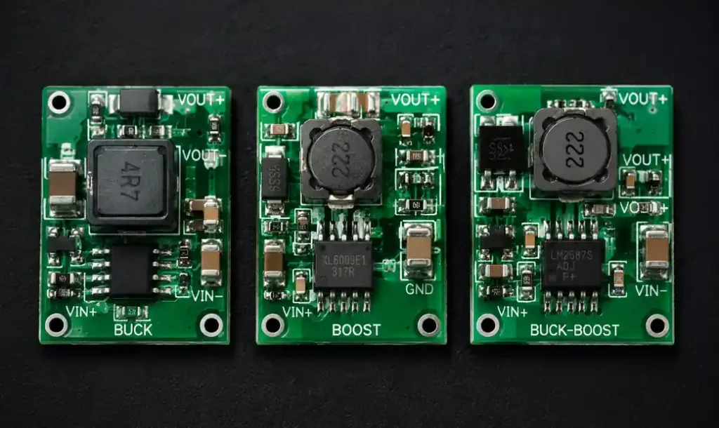
Before diving into layout specifics, let’s establish the fundamental differences between buck, boost, and buck-boost topologies and their PCB implications.
Buck Converters: Step-Down Topology
Buck converters reduce input voltage to a lower output voltage with high efficiency. The switching node connects directly to the inductor, creating a high-frequency square wave that demands careful routing. Input capacitors must handle pulsed currents at the switching frequency, typically 300kHz to 2MHz in modern designs.
Boost Converters: Step-Up Topology
Boost converters elevate voltage from input to output. Unlike buck converters, the output capacitor experiences pulsed charging currents, shifting the critical layout focus. The inductor connects between input and switching node, creating different electromagnetic field patterns that influence component placement.
Buck-Boost Converters: Bidirectional Capability
Buck-boost topologies handle both step-up and step-down conversion, making them ideal for battery-powered systems where input voltage varies across the battery discharge curve. Four-switch buck-boost designs offer superior efficiency but demand more complex PCB layouts due to additional switching nodes.
Critical Layout Principles for All Topologies
Minimizing Hot Loop Area
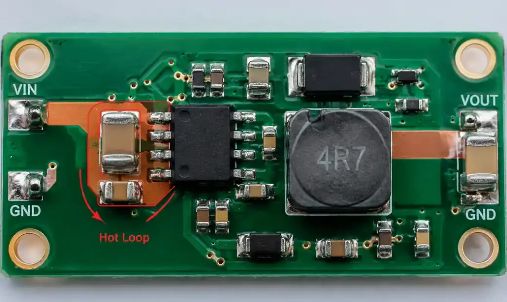
The hot loop—the high-frequency AC current path through input capacitor, switching FETs, and the circuit—creates the primary source of electromagnetic interference. Research from Analog Devices demonstrates that hot loop optimization can reduce radiated emissions by 15-20 dB.
For buck converters, the hot loop runs from input capacitor positive terminal, through the high-side FET, to the low-side FET, and back through the capacitor negative terminal. Place input capacitors within 5mm of the VIN and GND pins with copper traces as wide and short as possible.
In boost converters, the critical loop involves the low-side switch and output capacitor. Position output capacitors immediately adjacent to the switch node and output terminals.
Ground Plane Strategy
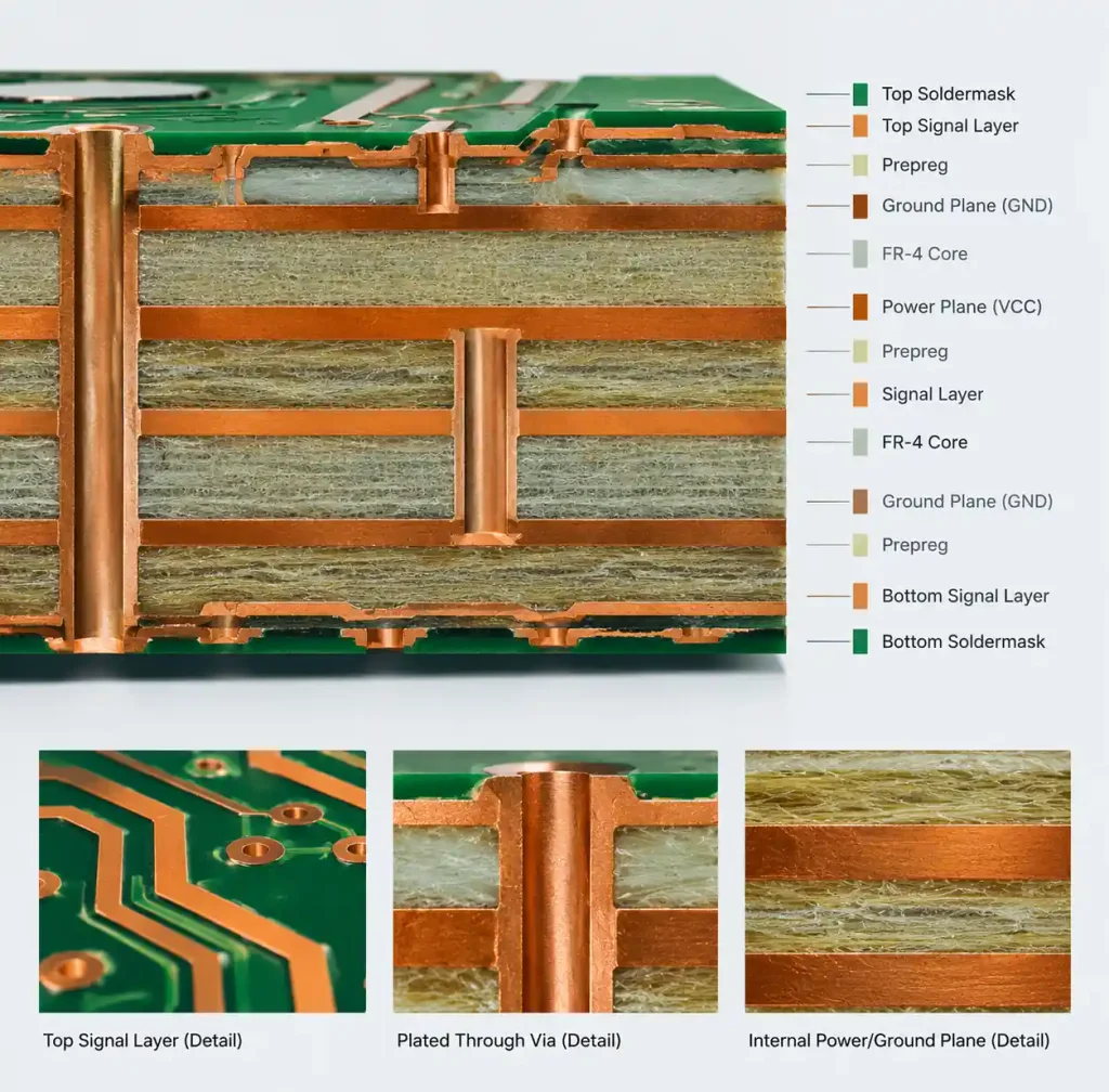
Multi-layer boards with dedicated ground planes offer substantial EMI reduction, but implementation details matter. Place the ground plane on layer 2 (immediately below the power components on layer 1) to provide the shortest return path for high-frequency currents.
Never split the ground plane beneath the power stage. While analog designers often separate analog and digital grounds, power converter layouts demand a continuous, low-impedance return path. Connect separate ground regions at a single star point near the power ground reference.
Buck Converter Layout Optimization
Component Placement Sequence
Start by placing the IC, then position components in this order based on current magnitude and frequency content:
- Input capacitor (directly at VIN pin within 2-5mm)
- Bootstrap capacitor (at BOOT pin)
- Output inductor (minimize trace length to SW pin)
- Output capacitor (near inductor, with ground vias)
- Feedback resistor network (route away from switching node)
Trace Width Calculations
Input and output current-carrying traces require careful sizing. For a 3A buck converter, minimum trace widths should be:
- VIN to input capacitor: 40 mils (1mm) for 2oz copper
- SW node to inductor: 30 mils (0.76mm)
- Inductor to output capacitor: 40 mils (1mm)
- GND return paths: 60 mils (1.5mm) minimum
Switching node traces should be kept short—under 10mm ideally—even if this requires slightly wider traces elsewhere.
Via Placement and Thermal Management
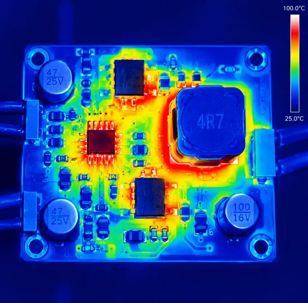
Place multiple ground vias (minimum 4-6) directly beneath the IC’s exposed thermal pad. Use 12-mil (0.3mm) vias with 0.5mm spacing to create an effective thermal and electrical connection to the ground plane. At Andwin Circuits, we’ve measured 15-20°C temperature reduction with properly designed thermal via arrays compared to inadequate thermal connections.
Boost Converter Specific Layout Techniques
Input Inductor Considerations
In boost topology, the inductor experiences continuous current flow, but the output capacitor sees high-frequency pulsed charging. This reversal of critical current paths compared to buck converters changes layout priorities.
Position the inductor between input and switching node with minimal trace inductance. Unlike buck converters where the inductor is on the output side, boost inductor placement directly impacts input current ripple and efficiency.
Output Capacitor Bank Design
Output capacitors in boost converters handle significantly higher RMS currents than buck outputs. For a 5V to 12V boost at 2A output, RMS capacitor current can exceed 3A. Use multiple ceramic capacitors in parallel:
- 3x 22µF X7R capacitors (minimum)
- Place within 3mm of VOUT pin
- Distribute around the IC for balanced current sharing
- Connect all negative terminals to a common ground point
Buck-Boost Layout Strategy
Four-Switch Topology Complexity
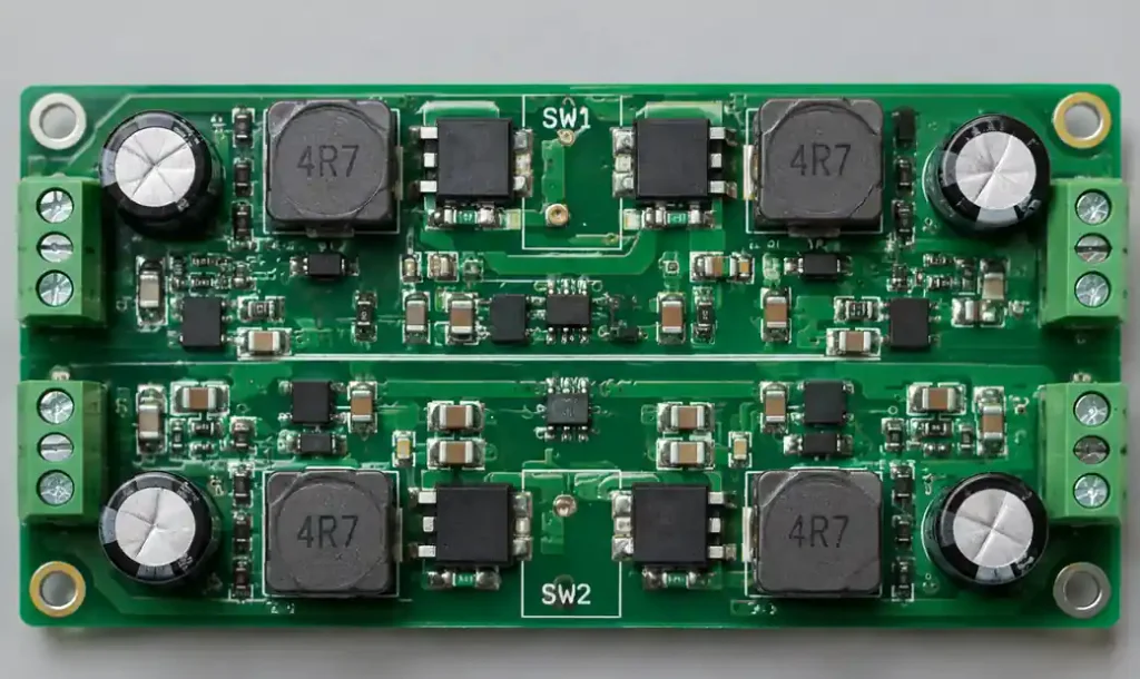
Four-switch buck-boost converters present unique challenges with two switching nodes simultaneously operating. The layout must minimize coupling between SW1 and SW2 while maintaining tight hot loops for both switching cells.
| Topology | Critical Loop | Maximum Loop Area | Primary EMI Source |
|---|---|---|---|
| Buck | Input cap → High/Low FETs → GND | < 100mm² | Input side switching |
| Boost | SW node → Output cap → GND | < 150mm² | Output side switching |
| Buck-Boost | Dual loops at SW1 and SW2 | < 80mm² each | Both switching nodes |
Managing Dual Switching Nodes
Separate SW1 and SW2 routing by at least 5mm to minimize capacitive coupling. Route feedback sensing from the output capacitor, avoiding proximity to either switching node. Shield sensitive analog traces with grounded copper fills on the same layer, connected to ground with multiple vias.
At switching frequencies above 1MHz, even 10mm of separation may be insufficient. Consider splitting the power stage across opposite sides of the PCB or using a stripline configuration with switching nodes on inner layers.
Layer Stack-Up Recommendations
Four-Layer Standard Configuration
For most DC-DC converter applications, a four-layer stack provides optimal performance:
- Layer 1 (Top): Power components, switching nodes, input/output traces
- Layer 2: Continuous ground plane (no splits beneath power stage)
- Layer 3: Analog signals, feedback routing, low-speed control
- Layer 4 (Bottom): Secondary power distribution, additional ground
This configuration places high-frequency return currents on Layer 2, immediately beneath their source traces, minimizing loop inductance and radiated emissions.
Six-Layer High-Performance Design
Applications requiring ultra-low noise or handling >10A benefit from six layers:
- Signal and low-current power
- Ground plane
- Power plane (VIN distribution)
- Power plane (VOUT distribution)
- Ground plane
- Signal and heat-spreading copper
Comparison of Converter Topologies for PCB Design
| Parameter | Buck Converter | Boost Converter | Buck-Boost Converter |
|---|---|---|---|
| Layout Complexity | Moderate | Moderate | High |
| Critical Capacitor | Input | Output | Both input and output |
| Hot Loop Location | Input side | Output side | Dual locations |
| Typical Efficiency | 90-95% | 85-92% | 85-93% |
| PCB Area (relative) | 1.0x | 1.1x | 1.4-1.8x |
| EMI Sensitivity | Medium | High | Highest |
| Thermal Hotspot | High-side FET | Inductor & switch | Multiple FETs |
Advanced Layout Techniques
Kelvin Sensing Connections
For precision voltage regulation, implement Kelvin (4-wire) sensing at the output. Run separate sense traces directly from the feedback pin to the output capacitor terminals, not from the main power traces. This eliminates IR drops in power traces from affecting regulation accuracy.
Route feedback traces on inner layers when possible, with ground plane shielding above and below. Maintain minimum 20-mil (0.5mm) spacing from switching nodes and high-current traces.
Copper Pour and Heat Spreading
Large copper areas aid thermal management but can increase capacitive coupling to switching nodes. Balance thermal needs with EMI considerations:
- Use hatched/crosshatched fills near switching nodes (reduce coupling)
- Solid copper pours for output regions (enhance cooling)
- Top and bottom layer copper pours connected with thermal vias
- Minimum 2oz (70µm) copper for power traces in >3A designs
Common Layout Mistakes and Solutions
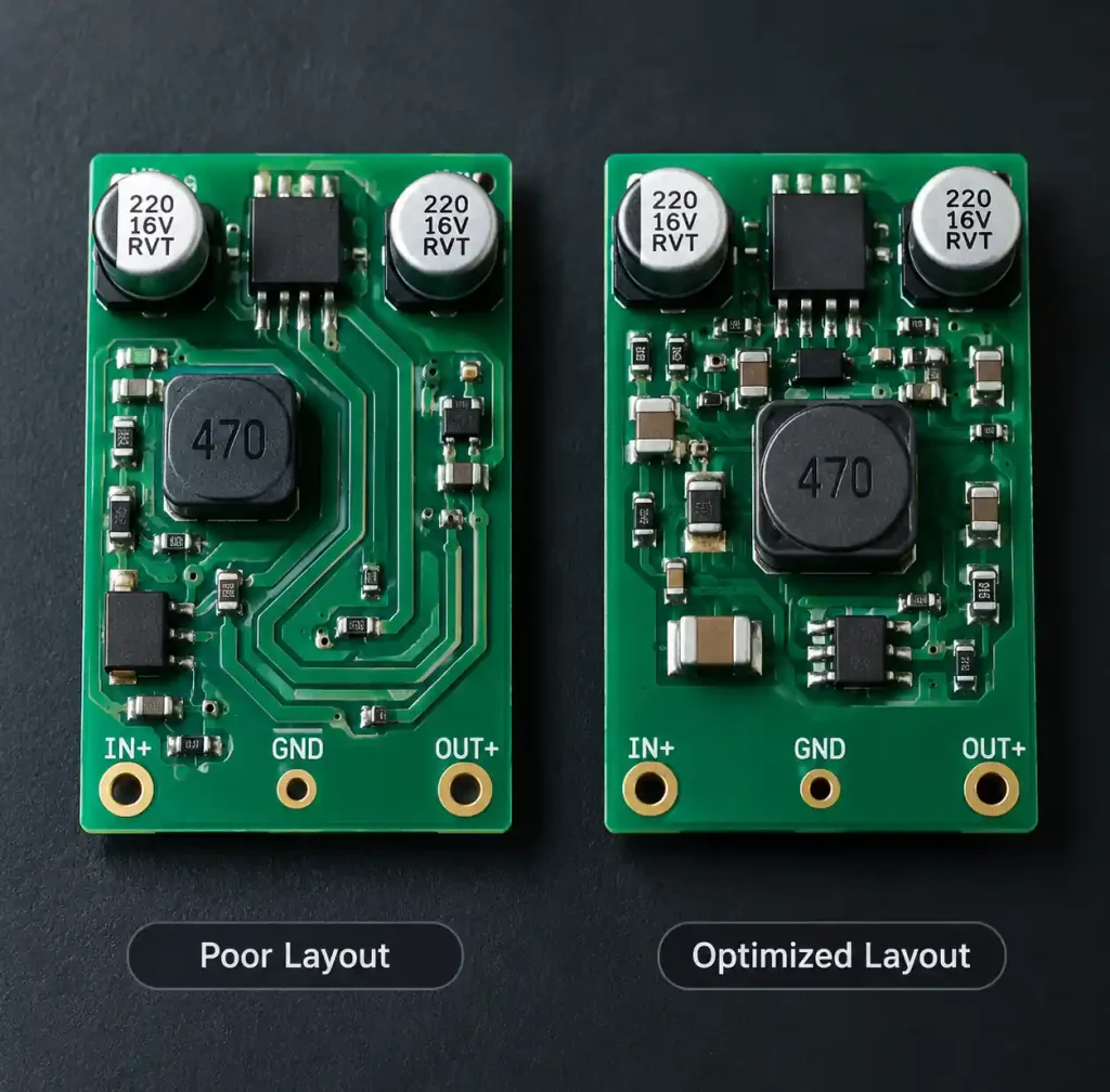
After reviewing hundreds of converter designs, these mistakes appear repeatedly:
Mistake: Placing input capacitor >10mm from VIN pin
Solution: Redesign component placement to achieve <5mm distance, even if this requires moving other components
Mistake: Single via for ground connections
Solution: Use via arrays: minimum 4 vias for signal grounds, 8-12 vias for power grounds
Mistake: Routing feedback traces parallel to switching node
Solution: Route perpendicular to switching nodes, use ground fill shielding
Mistake: Inadequate thermal vias under IC
Solution: Fill entire thermal pad area with 0.3mm vias at 0.5mm pitch
Testing and Validation
Pre-Production Verification
Before committing to volume production, validate critical layout parameters:
- Hot loop inductance: Target <10nH for 1MHz switching, <5nH for 2MHz
- Ground impedance: <5mΩ from IC ground to bulk capacitor ground at 1MHz
- Thermal resistance: Junction-to-ambient <40°C/W for typical SOIC packages
- EMI pre-compliance: Conducted emissions below CISPR 25 limits with 6dB margin
Andwin Circuits provides pre-production prototyping with same-day feedback on layout-related performance issues. Our engineering team reviews thermal imaging, current distribution analysis, and EMI scanning before production commits.
Real-World Performance Metrics
We recently completed a 12V to 5V/6A buck converter design where layout optimization improved:
- Efficiency: 88% → 94% at full load
- Peak switching node ringing: 3V → 0.8V
- Output ripple: 45mV → 12mV
- EMI failures: 4 frequency points → full compliance
These improvements came entirely from layout changes—no schematic modifications.
FAQ
Q: Can I use a two-layer PCB for DC-DC converters?
A: Two-layer designs work for low-power (<2A) converters with switching frequencies below 500kHz. However, ground plane benefits of four-layer boards typically justify the modest cost increase. For any design above 2A or 1MHz switching, use four layers minimum.
Q: How do I determine the optimal via size for thermal management?
A: Use 12-mil (0.3mm) finished hole diameter as a standard. Smaller vias (8-mil) increase manufacturing cost without thermal benefit. Larger vias (16-mil) consume excessive board area. Place vias at 0.5-0.7mm pitch to balance thermal performance and board density.
Q: Should switching node traces be kept on the top layer?
A: Yes, maintain switching nodes on the top layer where possible. Vias in switching node paths add inductance and create additional EMI coupling points. If you must transition layers, place the via immediately at the switching pin to minimize trace length on the top layer.
Q: What copper weight should I specify for power converter PCBs?
A: Standard 1oz (35µm) copper handles up to 2-3A per 40-mil trace. For 3-5A applications, specify 2oz (70µm) copper on outer layers. Above 5A, consider 2oz on all layers or local copper thickening in high-current regions.
Q: How close can I place other circuits to a DC-DC converter?
A: Maintain minimum 10mm clearance between power stage components and sensitive analog circuits. Digital circuits can be closer (5mm) as they have higher noise immunity. If board space is constrained, use grounded copper barriers between sections.
Q: Does inductor orientation affect PCB performance?
A: Yes. Orient shielded inductors with their magnetic field perpendicular to sensitive traces. For unshielded inductors, position them so magnetic flux lines run parallel to the PCB surface, minimizing coupling to traces beneath.
Conclusion
Successful PCB layout for buck, boost, and buck-boost converters depends on understanding the unique current paths and EMI sources in each topology. The fundamental principles—minimize hot loop area, provide low-impedance ground returns, and separate switching nodes from sensitive signals—apply universally, but implementation details vary significantly between topologies.
Buck converters demand careful input capacitor placement and switching node routing. Boost converters shift critical attention to output capacitor design and inductor positioning. Buck-boost designs require managing dual switching nodes while maintaining tight loops for both cells.
Whether you’re designing a simple 3.3V regulator or a complex battery management system, layout decisions made early in the design process determine final performance. Partner with experienced PCB manufacturers like Andwin Circuits who understand power converter requirements and can provide design feedback before production. Our team has optimized thousands of converter layouts, and we’re ready to help ensure your design meets performance, EMI, and thermal requirements from the first prototype.