
PCB for Motor Drives: High-Current Gate Driver Layout
Motor drive applications demand precise PCB design where gate driver layout directly impacts switching performance, efficiency, and EMI compliance. After designing over 200 motor controller boards, I’ve learned that successful high-current layouts stem from understanding parasitic inductance management rather than simply widening copper traces.
Why Gate Driver Layout Matters in Motor Drives
The gate driver circuit acts as the critical interface between your control logic and power MOSFETs or IGBTs. In motor drive applications operating at 20-100 kHz switching frequencies with load currents exceeding 50A, poor gate driver layout creates three immediate problems:
Parasitic inductance in the gate loop causes voltage overshoot during switching transitions. Each nanohenry of inductance generates approximately 1V of overshoot per ampere of di/dt during turn-on. For SiC MOSFETs with dV/dt exceeding 50V/ns, gate loop inductance must stay below 5nH to prevent cross-conduction.
Ringing and oscillation occur when gate loop inductance resonates with the MOSFET input capacitance. This creates high-frequency oscillations that radiate EMI and can trigger false turn-ons in the complementary switch of an H-bridge configuration.
Ground bounce from shared return paths allows switching noise to couple into the control circuitry, corrupting PWM signals and potentially causing shoot-through conditions.
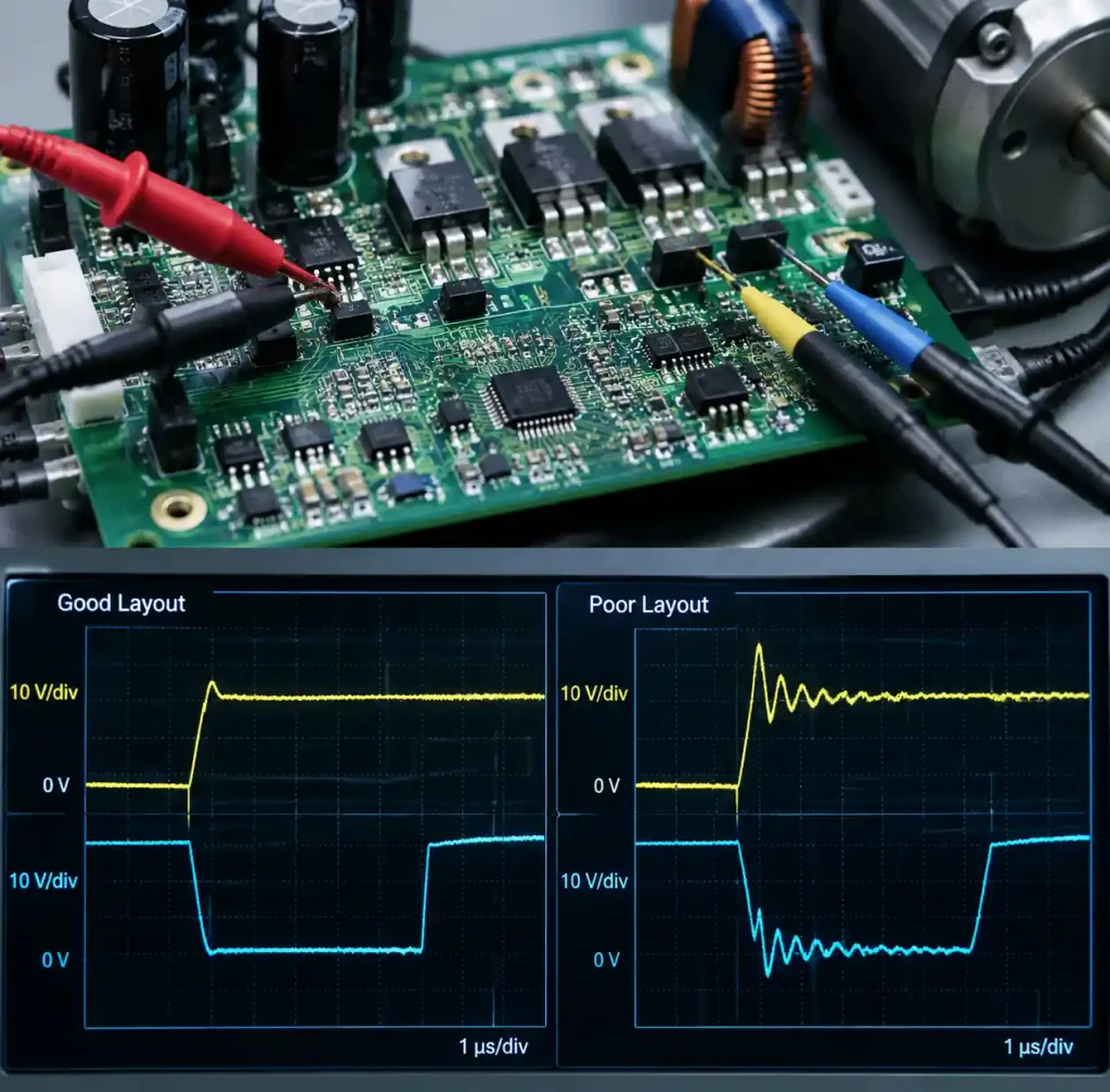
Critical Current Loops in Gate Driver Circuits
Understanding current flow paths reveals where layout attention delivers maximum impact. Motor drive gate circuits contain three distinct current loops, each requiring specific layout treatment:
High-Frequency Gate Charging Loop
This loop carries the highest frequency content, typically 10-50 MHz depending on gate resistor values and MOSFET capacitance. Current flows from the gate driver output, through the gate resistor, into the MOSFET gate capacitance, and returns through the driver ground pin.
Loop area must be minimized below 100mm² to maintain inductance under 10nH. Position the gate driver IC within 15mm of the power MOSFET, with the gate resistor placed directly adjacent to the MOSFET gate pin. Route the return path as a wide, short trace or solid pour directly back to the driver ground pin.
Driver Supply Decoupling Loop
Gate drivers source peak currents of 2-4A during switching transitions, even though average current remains under 100mA. This current pulse comes from the local decoupling capacitor, not the main power supply.
Place a 100nF ceramic capacitor (X7R or X5R dielectric) within 5mm of the driver VDD and GND pins. For drivers switching large MOSFETs (>10nC gate charge), add a 1µF bulk capacitor within 10mm. The decoupling loop area should not exceed 50mm².
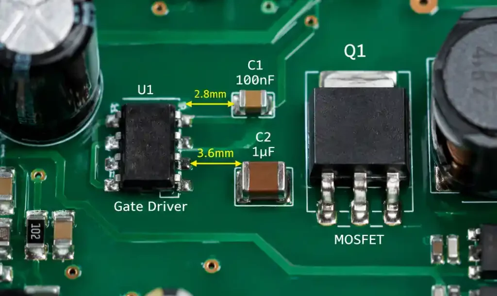
Bootstrap Circuit Loop (for High-Side Drivers)
Bootstrap circuits require special attention because the return path shifts with each switching cycle. The bootstrap capacitor charges through a diode when the low-side device conducts, creating a current loop that includes the power MOSFET source terminal.
Route the bootstrap diode and capacitor adjacent to the driver bootstrap and phase pins, maintaining loop area under 75mm². Use a 100nF fast-recovery diode rated for twice the bus voltage with sub-50ns reverse recovery time.
Power Stage Layout Fundamentals
The power stage switching loop represents the highest current (10-200A) and generates the strongest EMI. While not technically part of the gate driver, power stage layout directly affects gate driver performance through shared ground impedance and radiated coupling.
Minimizing Switching Loop Inductance
The critical path runs from the DC link capacitor positive terminal, through the high-side MOSFET, through the low-side MOSFET, and returns to the capacitor negative terminal. Every nanohenry in this loop generates voltage overshoot that the gate driver must suppress.
| Layout Parameter | Target Value | Impact if Exceeded |
|---|---|---|
| Loop area | <500mm² for <50A, <300mm² for >50A | 1V overshoot per 100mm² excess |
| Trace inductance | <10nH total | Increased switching loss, higher EMI |
| Capacitor ESL | <5nH | Reduced decoupling effectiveness |
| Phase node area | <100mm² | Increased radiated EMI |
Place DC link capacitors (minimum 470µF total, low-ESR aluminum or film) as close as possible to the power MOSFETs. For three-phase motor drives, position capacitors symmetrically to equalize inductance across all phases within 10%.
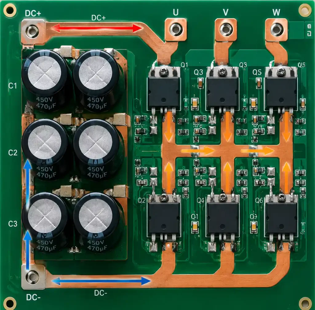
Copper Weight and Thermal Management
High-current motor drives require 2oz (70µm) copper minimum for power traces, with 3-4oz copper preferred for continuous currents above 30A. However, copper weight alone doesn’t ensure adequate current capacity – trace width and thermal vias matter equally.
Current capacity depends on allowable temperature rise. A 10mm wide trace in 2oz copper carries approximately 5A per layer with 10°C rise in still air. For 50A motor phase currents, parallel multiple layers or increase copper weight to 3-4oz.
Thermal vias under power MOSFETs transfer heat to internal copper planes or bottom-side thermal pads. Use arrays of 0.3mm vias spaced 0.8mm center-to-center, achieving thermal resistance under 1°C/W to a 4-layer board’s internal ground plane.
Layer Stack and Ground Architecture
Four-layer boards provide the minimum structure for reliable motor drive designs above 500W output power. Six layers become necessary above 2kW or when EMI compliance requires additional shielding.
Optimal Four-Layer Stack
From top to bottom:
- Top (signal + gate drives) – Component side with gate drivers, control circuits, and small signal traces
- GND (solid plane) – Continuous ground reference for return currents
- PWR (power distribution) – DC bus and motor phase routing, may be partially poured
- Bottom (power devices) – Power MOSFETs, current sensors, connectors
This stack places a solid ground plane immediately beneath the gate driver components, providing low-inductance return paths. The power layer on layer 3 allows controlled impedance routing for high-current paths while maintaining separation from sensitive gate signals.
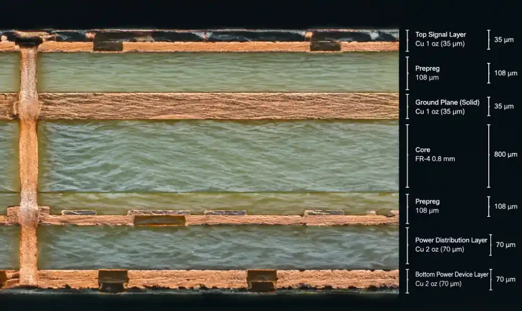
Ground Separation Strategy
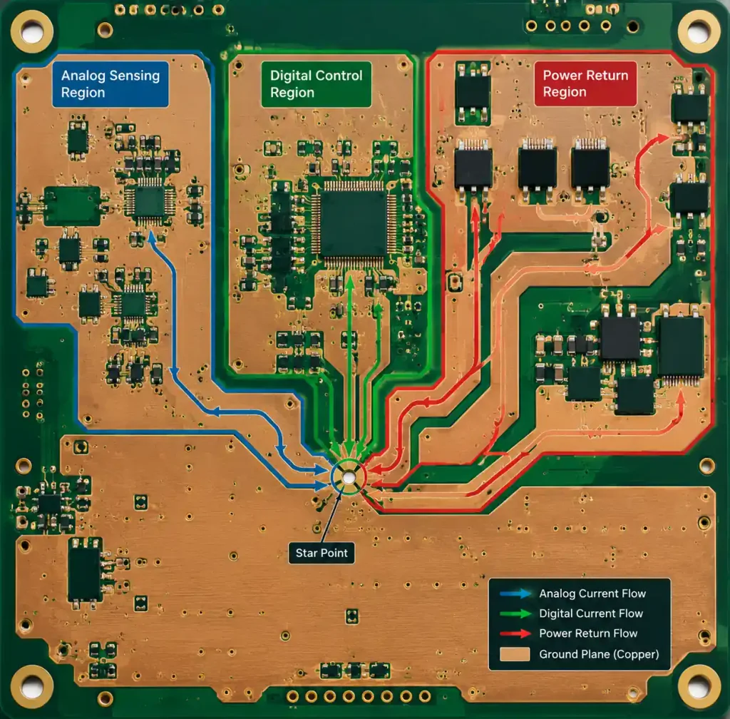
Motor drive boards require careful ground architecture to isolate analog, digital, and power return currents. However, contrary to outdated advice, splitting ground planes creates more problems than it solves in high-frequency circuits.
Use a single, continuous ground plane on layer 2 but control current return paths through component placement and trace routing. Position components so their associated return currents flow in defined regions without crossing sensitive areas.
| Circuit Type | Ground Strategy | Connection Point |
|---|---|---|
| Analog sensing | Route signals over analog region of ground plane | Star point at ADC or controller |
| Digital control | Route over digital region | Controller ground pins |
| Gate drivers | Dedicated return traces to driver ground pins | Power ground at MOSFET source |
| Power stage | Low-impedance plane connection | DC link capacitor negative terminal |
| Isolated power supplies | Separate islands connected only at transformer | No direct connection |
Connect analog, digital, and power ground regions together at a single star point, typically at the microcontroller or DSP ground pin. Some designs benefit from a 0Ω resistor or ferrite bead at this junction for measurement and optional filtering.
Component Placement Strategies
Physical component arrangement determines current loop geometry more than trace routing. Establish placement before routing any traces.
Gate driver positioning: Place each gate driver IC within 15mm of its corresponding power MOSFET. For half-bridge configurations, the driver should sit between the high-side and low-side devices, equidistant from both gates.
Decoupling capacitor proximity: The 100nF ceramic capacitors must be the closest components to each IC’s power pins, positioned within 5mm. Bulk capacitors (1-10µF) can sit 5-15mm away, typically sharing space with other bulk capacitance.
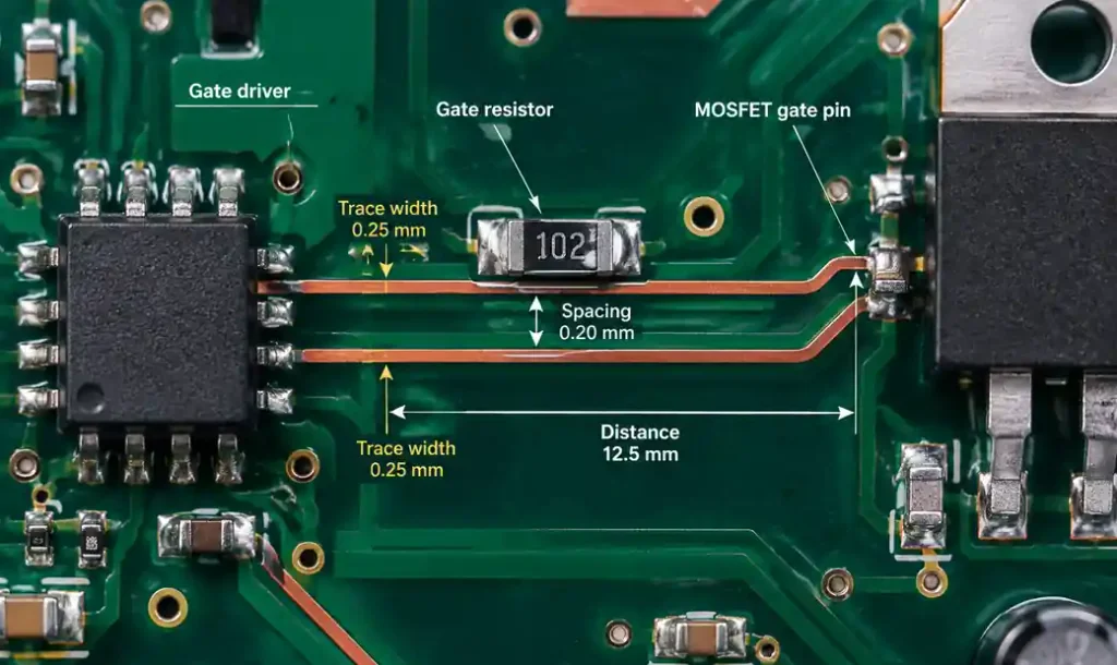
Gate resistor placement: External gate resistors should be placed within 3mm of the MOSFET gate pin, not at the driver output. This minimizes inductance in the high-frequency gate loop. For split gate resistors (different values for turn-on and turn-off), place both resistors at the MOSFET gate terminal.
Power MOSFET orientation: Orient MOSFETs to minimize the physical distance between drain terminals (for half-bridge configurations) and between source terminals and the gate driver ground. For packages with exposed thermal pads, orientation also affects thermal via placement.
Critical Trace Routing Techniques
After component placement establishes loop geometry, trace routing completes the current paths while managing impedance and EMI.
Gate Drive Signal Routing
Gate traces from the driver to the MOSFET gate pin should be short (under 30mm), direct, and maintain controlled impedance. For isolated gate drivers with >100mm routing distance, treat gate signals as transmission lines requiring impedance matching.
Width: 0.3-0.5mm (12-20mil) for typical gate drives with 5-10Ω series resistance. Wider traces reduce resistance but increase capacitance and EMI coupling.
Ground clearance: Maintain 0.5mm clearance from the gate trace to any ground plane beneath it. This controlled spacing creates a microstrip transmission line with ~50-70Ω impedance when the ground plane is on layer 2.
Return path: Route the gate driver ground return as a trace (not just relying on planes) when the gate current exceeds 2A peak. This 0.5-1mm trace should run parallel to the gate signal trace, maintaining less than 3mm separation. This creates a low-inductance differential pair that minimizes loop area.
Kelvin Connections for Current Sensing
Motor drives typically measure current using shunt resistors or MOSFET Rds(on) sensing. Accurate measurement requires Kelvin connections that isolate the sense path from power current.
For shunt resistors, route four separate traces: two carrying power current (wide, high-current traces) and two sensing voltage (narrow, low-current traces). The sense traces connect directly to the shunt resistor terminals at points separate from the power connections. This four-wire connection eliminates voltage drop in the power traces from corrupting the measurement.
EMI Mitigation Through Layout
Motor drives generate substantial conducted and radiated EMI due to fast switching edges and high di/dt currents. Layout techniques provide the first line of defense before resorting to external filters.
Shielding High dV/dt Nodes
The motor phase outputs (switching nodes) experience voltage slew rates of 10-100V/ns in typical PWM motor drives. These high dV/dt nodes couple capacitively to nearby circuits and cables, generating common-mode EMI.
Minimize exposed copper area at switching nodes to under 100mm² by routing motor phase traces as narrow, short connections to the output connector. Avoid unnecessary pads, test points, or filled regions connected to phase nodes.
Guard rings around switching nodes provide optional additional isolation. Route a grounded trace or fill around the phase node area, separated by 2-3mm. This intercepts electric field lines before they reach sensitive circuits.
Shielding layers in six-layer boards can be connected to ground and positioned between the switching node layer and sensitive signal layers, providing capacitive shielding.
Reducing Loop Radiation
Current loops act as antennas with radiated power proportional to loop area times current squared times frequency squared. The three loops discussed earlier (gate charging, decoupling, and power switching) all contribute to radiation.
For three-phase motor drives, maintain symmetry across all three phase legs to balance EMI generation. Asymmetrical layouts cause one phase to generate more EMI, complicating filter design.
Advanced Techniques for High-Performance Drives
Modern motor drives pushing toward higher power density and efficiency require additional layout refinement beyond the fundamentals.
Active Switching Node Clamping
SiC and GaN power devices with extremely fast switching speeds (>50V/ns) benefit from active clamping circuits that limit overshoot while maintaining low switching losses. These circuits require dedicated layout consideration.
RC snubbers across power devices must use low-inductance capacitors (<5nH ESL) placed within 10mm of the MOSFET drain and source terminals. Film or C0G ceramic capacitors work best. The resistor should be positioned between the capacitor and drain, minimizing inductance in the critical capacitor-to-MOSFET loop.
Active clamp circuits using additional MOSFETs or diodes require the same loop area minimization as the main power stage. The clamp device should be positioned adjacent to the main MOSFET, with decoupling capacitors shared or independently placed depending on clamp topology.
Integrated Current Sensing
Modern motor drives increasingly use integrated current sense amplifiers or MOSFET drain-source voltage sensing for loss-less current measurement. These techniques demand careful layout to avoid noise corruption.
For amplifier-based sensing, route differential pairs from the shunt resistor to the amplifier inputs with <0.5mm separation, equal length within 2mm, and symmetric ground plane beneath both traces. This differential routing provides common-mode noise rejection.
Design Verification and Testing
Even with optimal layout, verification ensures the design meets performance targets before committing to manufacturing.
Simulation and Pre-Layout Analysis
Loop inductance extraction: Use 3D field solvers (ANSYS Q3D Extractor, COMSOL, or similar tools) to calculate inductance of critical current loops from preliminary layouts. Target values: gate loop <10nH, decoupling loop <5nH, power switching loop <15nH for half-bridge modules.
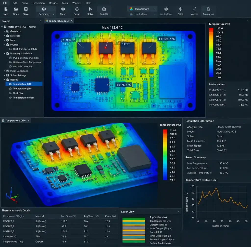
Thermal simulation: Model thermal performance using finite element analysis (FEA) to verify MOSFET junction temperatures remain below 125°C at maximum load. Tools like ANSYS Icepak or Simcad provide PCB-specific thermal modeling.
Post-Layout Verification
| Test Parameter | Measurement Method | Acceptance Criteria |
|---|---|---|
| Gate voltage rise/fall time | Oscilloscope at MOSFET gate pin | 10-50ns depending on gate resistor |
| Gate voltage overshoot | Oscilloscope, 500MHz bandwidth minimum | <10% of drive voltage |
| Drain-source voltage overshoot | Oscilloscope at MOSFET drain | <15% of bus voltage |
| Gate-source voltage ringing frequency | Oscilloscope FFT analysis | Match simulation within 20% |
| MOSFET junction temperature | Thermal camera or thermocouple | <125°C at rated current |
| Conducted EMI | EMI receiver with LISN, 150kHz-30MHz | Below regulatory limit -6dB |
Use a current probe with >50MHz bandwidth to measure actual current waveforms in critical loops. Compare measured loop inductance (from di/dt and voltage overshoot) against simulation to validate models.
Common Layout Mistakes and Solutions
Through years of debugging motor drive failures, certain layout errors appear repeatedly. Recognition enables prevention.
Mistake: Routing gate driver ground return through power ground plane without dedicated trace. This allows switching noise from the power stage to corrupt the gate signal through shared impedance.
Solution: Route a dedicated ground return trace from each driver ground pin to the power MOSFET source terminal, typically 0.5-1mm wide for 2-4A peak gate current.
Mistake: Placing gate resistors at the driver output instead of at the MOSFET gate. This separates the resistor from the point where damping is needed.
Solution: Position all gate resistors within 3mm of the MOSFET gate pin. For split resistors, place both at the gate terminal with minimal loop area for the turnoff path including the antiparallel diode.
Mistake: Using insufficient thermal vias under power devices or placing them only beneath the thermal pad center.
Solution: Create via arrays extending beyond the thermal pad by 2-3mm in all directions. Use 0.3mm vias on 0.8mm pitch for 4-layer boards, 0.6mm pitch for 6-layer boards with thicker copper.
Frequently Asked Questions
Q: What copper weight should I specify for motor drive PCBs carrying 50A phase currents?
For continuous 50A current, use 3oz (105µm) copper minimum on power traces, with 2oz adequate for layers carrying return currents. Calculate required trace width using IPC-2221 standards allowing 10-20°C temperature rise. A 10mm wide trace in 3oz copper carries approximately 12-15A with 10°C rise, so 50A requires parallel routing across multiple layers or wider traces (15-20mm).
Q: Can I use a two-layer PCB for motor drives under 1kW output power?
Two-layer designs work for lower-power applications (<500W) if you accept compromises in EMI performance and thermal management. You must route return currents very carefully since no solid ground plane exists. Consider four-layer construction as the minimum for reliable designs, especially if EMI compliance is required.
Q: How close should the DC link capacitor be placed to the power MOSFETs?
Physical proximity matters less than loop inductance. Target capacitor terminal-to-MOSFET terminal distance under 30mm with wide, short traces creating loop area under 500mm². Multiple smaller capacitors distributed across the power stage often outperform one large centralized capacitor.
Q: Should I split the ground plane between analog and power sections?
No. Ground plane splits create high-impedance gaps that high-frequency currents must cross, generating EMI and noise coupling. Use a continuous ground plane on layer 2, control return current paths through component placement and trace routing, and connect different ground regions at a single star point.
Q: What’s the maximum acceptable gate loop inductance for SiC MOSFETs?
SiC devices with their fast switching speeds require gate loop inductance below 5nH to prevent parasitic turn-on and excessive ringing. Achieve this through driver placement within 10-15mm of the MOSFET, minimizing gate resistor lead length, and providing dedicated ground return traces. Silicon IGBTs and older MOSFETs tolerate 10-15nH.
Q: Do I need separate gate resistors for turn-on and turn-off?
Split gate resistors (different values for turn-on versus turn-off) optimize switching performance by independently controlling rise time and fall time. Use separate resistors when turn-off speed must be faster than turn-on to prevent shoot-through in bridge configurations, or when EMI requirements demand slower turn-on with maintained turn-off speed for efficiency.
Conclusion
High-current gate driver layout for motor drives succeeds through systematic attention to parasitic management rather than arbitrary design rules. The three critical current loops – gate charging, driver decoupling, and power switching – each require specific loop area targets below 100mm², 50mm², and 500mm² respectively to maintain inductance under 10nH, 5nH, and 15nH.
Component placement establishes these loop geometries before routing begins. Gate drivers sit within 15mm of power MOSFETs, decoupling capacitors within 5mm of IC power pins, and DC link capacitors create short, wide connections to the power stage. A continuous ground plane on layer 2 of a four-layer stack provides low-inductance return paths while component arrangement controls current flow.
Successful motor drive PCB layout stems from understanding that every trace, via, and component placement decision affects multiple parameters simultaneously. The gate circuit layout influences switching speed, EMI generation, and efficiency. Power stage geometry determines voltage overshoot, thermal performance, and conducted noise. Ground plane architecture impacts both signal integrity and power quality. Master these interconnected relationships, verify with simulation and measurement, and your motor drive boards will deliver reliable performance from prototype through production.