
RF PCB Design: Microstrip vs Stripline for High-Frequency Circuits
RF engineers face a fundamental choice when routing signals above 1 GHz: microstrip or stripline transmission lines. This decision directly affects insertion loss, EMI performance, and impedance stability. Improper transmission line selection can cost 0.5-1.5 dB in insertion loss and create coupling issues that post-layout tuning cannot fix.
At 5 GHz, poorly chosen transmission line structure combined with wrong material selection accounts for 35% of first-pass failures. If you’re designing 1-10 GHz RF circuits for wireless, radar, or test equipment, understanding when to use microstrip versus stripline—and how to calculate impedance—determines whether your board works on first spin.
What Are Microstrip and Stripline Transmission Lines?
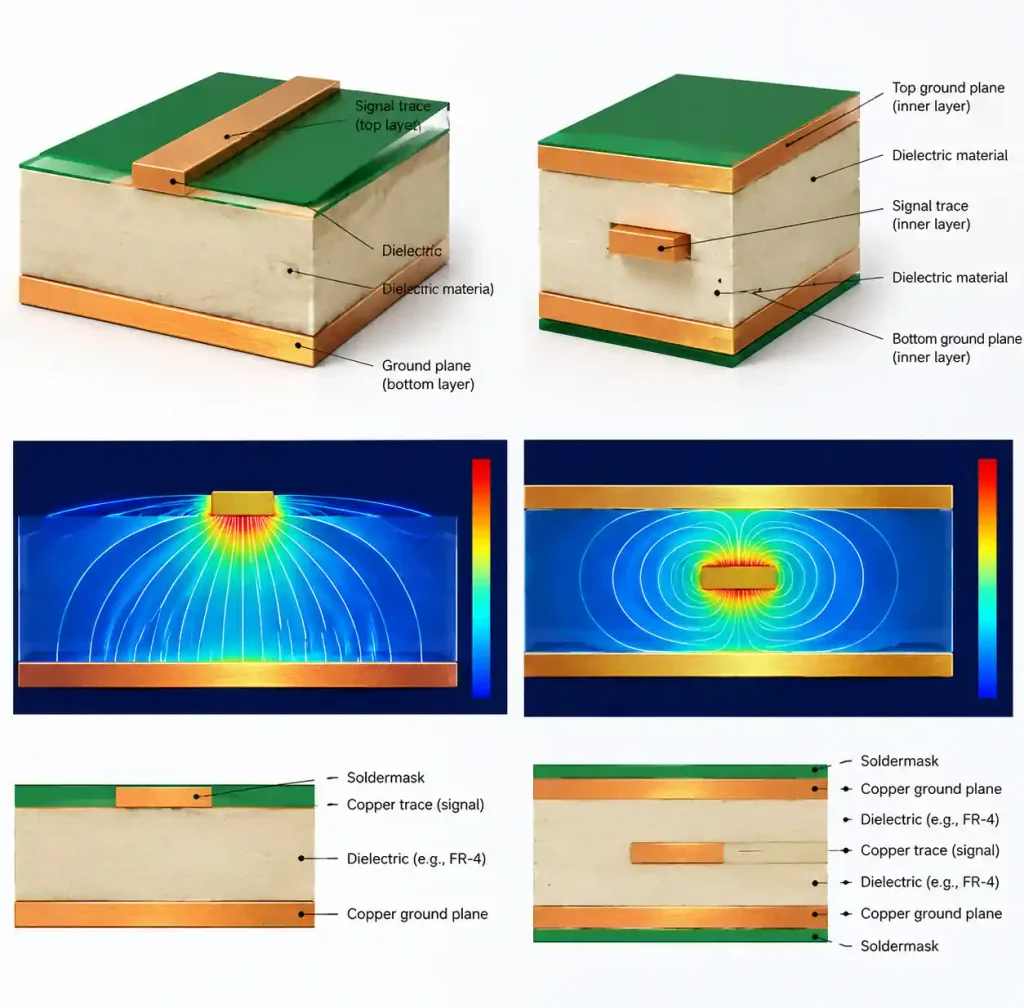
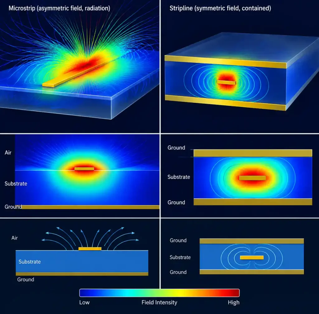
Microstrip consists of a signal trace on the outer PCB layer with a ground plane below. The field propagates partly through substrate and partly through air, creating an effective dielectric constant (εr_eff) lower than the substrate’s εr.
Stripline places the signal trace between two ground planes on internal layers. The field stays entirely within the dielectric, making εr_eff equal to substrate εr. This symmetric structure provides inherent shielding but requires minimum 4-layer stackup.
At 2.4 GHz in standard FR-4, wavelength is approximately 50mm. A 12mm trace becomes nearly quarter-wavelength—where impedance discontinuities create reflections degrading return loss below -10 dB.
Microstrip vs Stripline: Key Performance Comparison
| Parameter | Microstrip | Stripline |
|---|---|---|
| Insertion Loss at 5 GHz (RO4003C) | 0.15-0.25 dB/inch | 0.20-0.30 dB/inch |
| EMI Shielding | Minimal (radiates) | Excellent (20-30 dB better) |
| Minimum Layers | 2-layer works | Requires 4+ layers |
| Impedance Stability (Temp) | ±3-5% (-40°C to +85°C) | ±1-2% (-40°C to +85°C) |
| Component Mounting | Direct possible | No direct access |
| Fabrication Cost | Lower | 30-50% higher |
| Effective εr | 0.5-0.7 × substrate εr | Equal to substrate εr |
| Crosstalk (6-mil spacing) | -30 to -35 dB | -45 to -55 dB |
Microstrip delivers lower conductor loss with traces on outer layers where copper can exceed 1 oz. Stripline’s internal placement limits practical copper to 0.5-1 oz, increasing resistance.
However, stripline’s 20-30 dB better shielding makes it essential for sensitive receivers and multi-stage amplifiers where isolation prevents unwanted coupling. This crosstalk immunity often outweighs slightly higher conductor loss.
Impedance Calculation: Getting to 50Ω
Achieving 50Ω requires precise control of trace width, dielectric thickness, and copper weight. Calculations differ between microstrip and stripline due to field distributions.
Microstrip Impedance Formula
IPC-2141 simplified formula:
Z₀ = 87/√(εr + 1.41) × ln[5.98h/(0.8w + t)]
Where:
- Z₀ = characteristic impedance (Ω)
- εr = substrate dielectric constant
- h = dielectric thickness (mils)
- w = trace width (mils)
- t = copper thickness (mils)
Example for 50Ω microstrip on RO4003C (εr = 3.55):
- h = 8 mil, t = 1.4 mil (1oz copper)
- Result: w ≈ 16 mil (0.406mm)
On thicker 10-mil core, the 50Ω trace widens to approximately 20 mils. Always verify with your manufacturer’s impedance calculator before fabrication.
Stripline Impedance Formula
For stripline centered between ground planes:
Z₀ = 60/√εr × ln[4h/(0.67π(0.8w + t))]
Where h = distance from trace center to each ground plane.
Example for 50Ω stripline on RO4003C:
- Total thickness = 16 mil (8 mil each side)
- h = 8 mil, t = 1.4 mil, εr = 3.55
- Result: w ≈ 10 mil (0.254mm)
Stripline requires narrower traces than microstrip for same impedance because effective dielectric constant is higher.
Material Selection: Rogers vs FR-4 for RF
Material choice determines impedance stability across frequency and temperature. FR-4 works below 3 GHz for prototypes, but Rogers laminates provide superior performance for production RF boards.
| Property | FR-4 (Standard) | Rogers RO4003C | Rogers RO4350B |
|---|---|---|---|
| Dk (10 GHz) | 4.2-4.5 (±10%) | 3.55 (±2%) | 3.66 (±2%) |
| Loss Tangent (10 GHz) | 0.015-0.020 | 0.0027 | 0.0037 |
| CTE (ppm/°C) | 14-17 | 11-14 | 10-12 |
| Cost vs FR-4 | 1× | 3-4× | 3-4× |
| Frequency Range | Up to 2-3 GHz | Up to 10 GHz | Up to 10 GHz |
Loss tangent directly determines insertion loss. At 10 GHz over 100mm microstrip, FR-4 (Df 0.018) produces 0.8-1.0 dB loss, while RO4003C (Df 0.0027) yields only 0.4-0.5 dB—a 0.4-0.5 dB improvement critical for link budget-limited systems.
RO4003C balances performance with standard FR-4 processing equipment, reducing fabrication cost versus PTFE materials. For 1-6 GHz where loss budget allows, RO4350B provides similar performance with slightly higher dielectric constant.
Via Transitions: Microstrip-to-Stripline Design
Real RF layouts require layer transitions to reach components or cross dense routing. Via transitions introduce parasitic inductance and capacitance degrading performance if not properly designed.
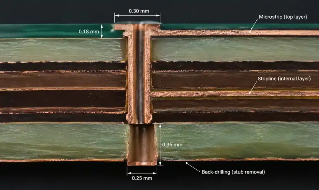
A through-via creates a stub—an unterminated transmission line that resonates at specific frequencies. At quarter-wave resonance, return loss degrades from -20 dB to -8 dB. For 62-mil thick board, first stub resonance occurs around 8-9 GHz.
Three mitigation techniques:
Back-drilling removes unused via stub below signal connection. Adds $150-300 per panel but pushes stub resonance above 15-20 GHz, making vias transparent below 10 GHz.
Via fencing surrounds signal vias with grounded vias spaced λ/10 (≈125 mils at 5 GHz on RO4003C). Provides low-impedance return path, improving return loss by 3-5 dB.
Blind/buried vias eliminate stubs by connecting only required layers. Best for high-speed PCB above 20 GHz but increases cost 20-40% versus back-drilling.
Back-drilling provides best cost-performance balance up to 10 GHz.
When to Use Microstrip vs Stripline
Selection depends on frequency, EMI requirements, and system architecture:
Choose Microstrip when:
- Operating below 6 GHz in shielded environments
- Board cost critical (2-layer possible)
- Direct component mounting needed
- Probing access required
Choose Stripline when:
- Operating above 6 GHz or dense layouts
- Crosstalk must stay below -40 dB
- Strict EMI limits
- RF gain blocks need isolation
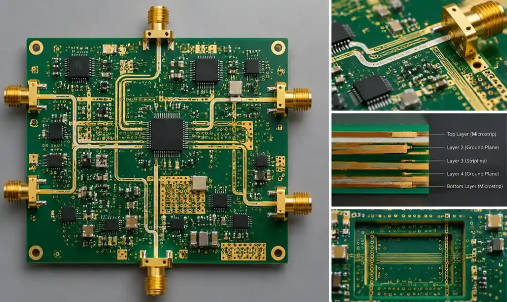
For mixed designs, use stripline for LNA inputs, LO distribution, and mixer paths. Route less critical signals on microstrip to save layers. Commercial WiFi modules often use hybrid approaches: microstrip for antenna feed (minimize loss), stripline for LO (prevent leakage).
EMI Characteristics and Design Guidelines
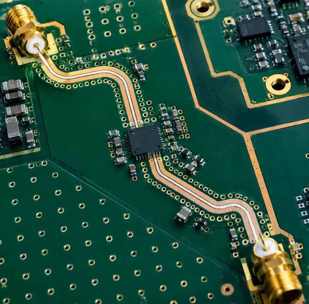
Microstrip’s asymmetric field radiates energy. At 5 GHz, a 50mm microstrip trace driven with 0 dBm radiates approximately -30 to -40 dBm—enough to fail FCC Part 15 Class B without shielding.
Stripline’s symmetric structure with dual ground planes provides 20-30 dB better containment. Radiated emissions typically run 25-35 dB lower than equivalent microstrip.
Three practices reduce microstrip EMI:
Ground plane stitching: Place grounded vias every λ/10 (≈125 mils at 5 GHz) around microstrip routing perimeters.
Keep-out zones: Maintain 5× trace width clearance between RF traces and board edges.
Shield can integration: For traces >+10 dBm, integrate grounded metal shield with via fencing (reduces emissions 30-40 dB).
Stripline requires less aggressive mitigation—ensure ground continuity with λ/10 via spacing and avoid routing near board edges.
Loss Analysis: 1-10 GHz Performance
Total insertion loss combines conductor loss, dielectric loss, and discontinuity losses. The dominant mechanism changes with frequency.
Below 3 GHz, conductor loss dominates. Skin depth at 2 GHz is approximately 1.5 μm. Standard electrodeposited copper (RMS ~5 μm) adds 15-25% more loss than rolled copper (RMS ~1 μm).
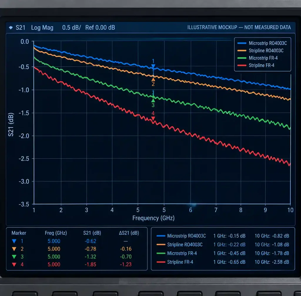
From 3-10 GHz, dielectric loss becomes dominant. RO4003C maintains Df below 0.003, while FR-4 increases from 0.015 at 1 GHz to 0.020+ at 10 GHz. Over typical 150mm trace at 10 GHz:
- Microstrip on RO4003C: 0.6-0.8 dB
- Stripline on RO4003C: 0.8-1.0 dB
- Microstrip on FR-4: 1.5-2.0 dB
- Stripline on FR-4: 1.8-2.5 dB
For link budget-limited systems, the 1-1.5 dB improvement from Rogers materials directly increases range by 12-18% or allows lower transmit power.
Field Solver Simulation Workflow
Field solvers validate impedance calculations and identify discontinuities before fabrication. Simulating actual stackup with manufacturing tolerances prevents costly respins.
Essential steps:
- Model actual stackup including tolerances: prepreg ±10%, copper ±10%, Dk variation (±2% Rogers, ±10% FR-4)
- Run corner cases combining worst-case tolerances
- Simulate via transitions including pad diameter, clearance, and stub length
- Add ground stitching to verify return loss improvement
Most manufacturers provide field solver files for standard stackups—use these as templates. Tools include Ansys HFSS, Keysight ADS Momentum, and Sonnet.
After simulation, fabricate impedance test coupons on production panels. Time-domain reflectometry (TDR) measurement provides ground truth for validating simulation and process control.
FAQ
What frequency is the threshold for choosing stripline over microstrip?
The threshold depends on EMI requirements, not just frequency. Use stripline above 6 GHz or when crosstalk must stay below -40 dB. For cost-sensitive products below 3 GHz in shielded enclosures, microstrip works. Sensitive receivers benefit from stripline at any frequency.
Can I use FR-4 material for RF designs at 5 GHz?
High-quality FR-4 (Dk tolerance ±5%, Df <0.012) works for prototypes below 3-5 GHz if you accept 0.5-1.0 dB higher loss and ±5% impedance variation. Designs requiring better than -15 dB return loss or operating above 5 GHz should use Rogers laminates.
How much does back-drilling improve via performance?
Back-drilling removes via stub resonance causing return loss degradation. Measurements show 5-8 dB improvement in S11 above 6 GHz. For 62-mil board, back-drilling pushes resonances from 8-9 GHz to above 15 GHz.
What trace width do I need for 50Ω impedance?
It depends on stackup. Microstrip on 8-mil RO4003C needs approximately 16 mils. Stripline on 16-mil total thickness needs approximately 10 mils. Never use rules of thumb—calculate for your actual stackup using impedance calculators and verify with test coupons.
Should I use GCPW instead of microstrip or stripline?
Grounded coplanar waveguide provides better mode control but requires careful stitching and wider channels. Use GCPW above 20 GHz, for connector transitions, or where probing matters. For 1-10 GHz routing, microstrip and stripline are simpler and more cost-effective.
Conclusion
Choosing between microstrip and stripline transmission lines determines RF PCB insertion loss, crosstalk immunity, and EMI performance. Microstrip offers lower conductor loss and simpler fabrication but radiates and couples more. Stripline provides superior shielding and impedance stability at the cost of additional layers.
Use Rogers RO4003C or RO4350B above 3 GHz, implement back-drilling for via transitions, and validate stackup with field solver simulation before fabrication. Choose microstrip for cost-sensitive surface routing below 6 GHz and stripline for sensitive paths requiring isolation better than -40 dB.
Andwin Circuits manufactures RF PCBs with microstrip and stripline controlled impedance using Rogers RO4000 series and FR-4 materials. Our process includes TDR impedance testing, back-drilling capability, and engineering support for stackup design. Contact us for RF PCB requirements with quick-turn prototyping and production volumes.