
Embedded Components in PCB: Technology Overview and Cost Analysis
Embedded component technology accounts for 15-20% of advanced PCB applications in mobile and automotive sectors. Industry data shows that proper implementation can reduce board size by 30-50% while cutting assembly costs by 20-35%. However, the technology demands precise process control and higher initial investment.
If you’re designing high-density electronics where board space directly impacts product cost and performance, understanding embedded components becomes essential. This guide breaks down the technology, manufacturing requirements, cost tradeoffs, and reliability considerations based on real production experience.
What Are Embedded Components in PCB?
Embedded components are passive or active electronic parts placed inside PCB layers rather than surface-mounted. The components sit within the board stackup—between copper layers—and connect through microvias or buried vias.
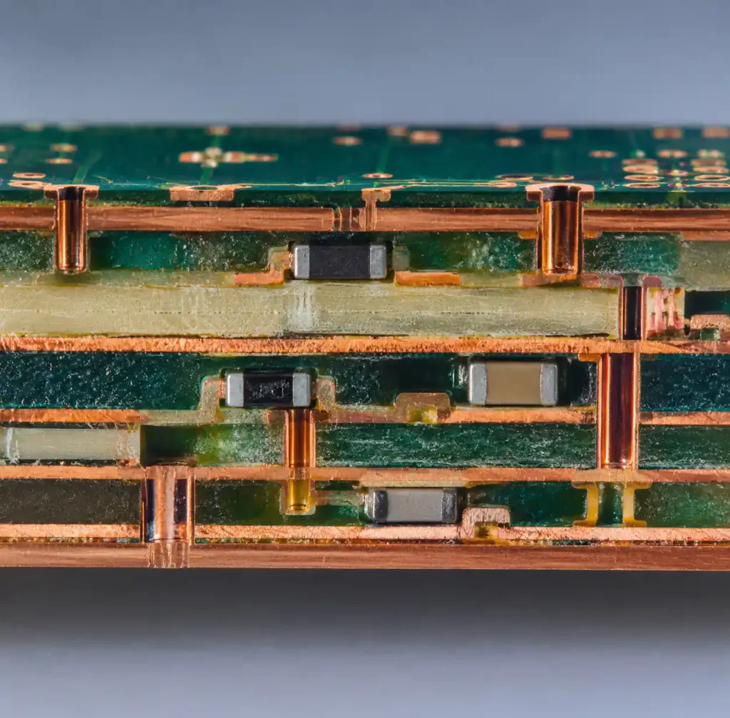
Key differences from surface mount:
- Components occupy internal layers, freeing surface area
- Shorter electrical paths reduce parasitic inductance and capacitance
- Protected from mechanical damage and environmental exposure
- Requires specialized lamination and laser drilling processes
The technology primarily targets passive components (resistors, capacitors) due to mature processes and lower risk. Active component embedding (ICs, dies) remains limited to specialized applications due to thermal management challenges and rework complexity.
Types of Embedded Components
Embedded Passive Components
Resistors:
- Resistive films deposited on dielectric layers
- Typical range: 10Ω to 1MΩ
- Tolerance: ±5% to ±20% depending on material
- Common materials: NiP (Nickel Phosphorus), carbon-based inks
- Sheet resistance: 25-100 Ω/square
Capacitors:
- High-k dielectric materials between copper layers
- Typical values: 10pF to 10nF
- Materials: barium titanate, epoxy-ceramic composites
- Dielectric constant (εr): 10-1000
- Voltage rating limited by layer thickness (typically 16-63V)
Inductors:
- Spiral traces embedded in inner layers
- Values: 1nH to 100nH
- Used primarily for RF impedance matching
- Quality factor (Q) lower than discrete components
Active Component Embedding
Die embedding:
- Bare IC dies placed in board cavities
- Wire bonding or flip-chip connections
- Applications: power management ICs, RF front-ends
- Major challenge: heat dissipation and thermal cycling stress
| Component Type | Maturity Level | Cost Premium vs SMT | Typical Applications |
|---|---|---|---|
| Embedded resistors | Production-ready | +15-25% | Power distribution, termination networks |
| Embedded capacitors | Production-ready | +20-30% | Decoupling, high-frequency filtering |
| Embedded inductors | Limited production | +25-40% | RF matching, EMI suppression |
| Embedded dies (active) | Prototyping/low volume | +50-100% | System-in-package, ultra-compact devices |
Manufacturing Process for Embedded Components
The fabrication process differs significantly from standard PCB manufacturing and requires additional equipment and process control.
Process Flow Overview
1. Core preparation:
- Start with thin core material (100-200μm)
- Deposit resistive or capacitive films
- Pattern using photolithography
- Laser ablation for precision features
2. Component placement (for discrete embedding):
- Create cavities using CNC routing or laser
- Place passive chips or dies
- Fill gaps with epoxy or resin
- Planarize surface through grinding
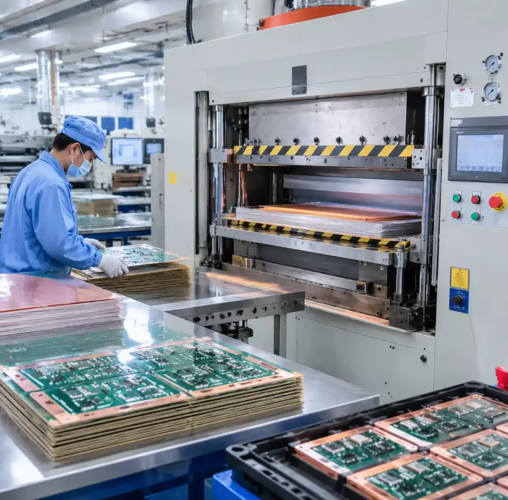
3. Lamination:
- Stack cores with prepreg layers
- Vacuum lamination cycle (critical for void prevention)
- Pressure: 300-400 psi
- Temperature: 170-200°C depending on materials
4. Via formation:
- Laser drilling for microvias to embedded components
- CO₂ or UV laser systems
- Typical via diameter: 75-150μm
- Aspect ratio limit: 1:1 for laser vias
5. Plating and finishing:
- Copper electroplating fills vias
- Standard PCB processing for outer layers
- Final thickness typically 1.0-1.6mm for 8-12 layer boards
Design Rules for Embedded Components
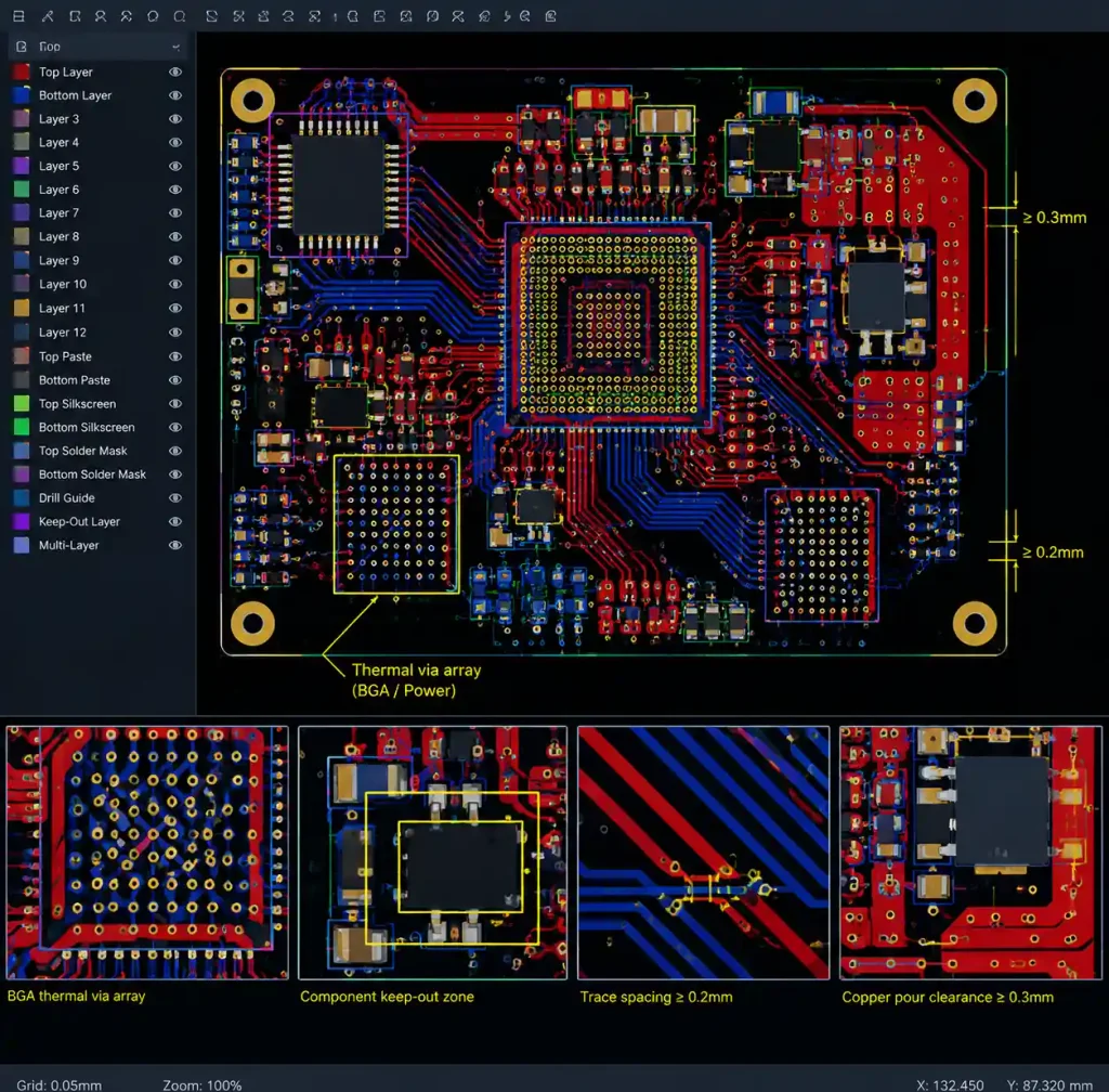
Spacing requirements:
- Minimum distance between embedded components: 0.5mm
- Clearance to board edge: ≥2mm
- Via-to-component spacing: ≥0.3mm
Thermal considerations:
- Thermal vias required for components >0.5W dissipation
- Via array density: 4-6 vias per cm² for heat spreading
- Copper planes above/below embedded components aid thermal management
Layer stackup:
- Place embedded passives in L3-L4 for 8-layer board
- Active components only in central layers (L4-L5 in 10-layer)
- Maintain symmetry to control warpage
Cost Analysis: Embedded vs Surface Mount
Direct Cost Comparison
| Cost Factor | Standard SMT | Embedded Components | Impact |
|---|---|---|---|
| Component cost | Baseline | -10 to -20% | Bulk material vs discrete parts |
| PCB fabrication | Baseline | +30 to +50% | Additional process steps |
| Assembly cost | Baseline | -15 to -25% | Fewer placement operations |
| Testing cost | Baseline | +10 to +20% | Limited access for rework |
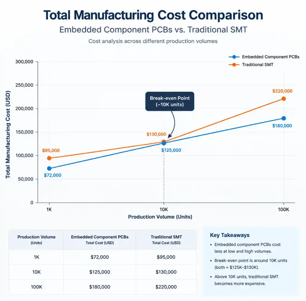
| Total manufacturing cost | 100% | 95-135% | Volume dependent |
Break-even analysis:
- Low volume (<1,000 units): 20-35% cost increase
- Medium volume (10,000 units): 5-15% cost increase
- High volume (>100,000 units): 0-10% cost savings
Hidden Cost Factors
Development costs:
- Design tool licenses for embedded component CAD: $5,000-15,000
- Prototype iteration cycles longer: 3-4 weeks vs 1-2 weeks for SMT
- First article testing more complex
Yield considerations:
- Embedded passive yield: 95-98% in production
- Active component embedding: 85-92% (thermal stress failures)
- Rework impossible for embedded components—scrapped boards
Long-term economics:
The technology makes financial sense when:
- Board space savings enable smaller product footprint (direct material cost reduction)
- Component count reduction simplifies supply chain
- Performance improvements (signal integrity, EMI) eliminate costly fixes
- High-volume production amortizes tooling costs
Performance Benefits and Trade-offs
Electrical Performance Gains
Reduced parasitic effects:
- Lead inductance eliminated: typical reduction from 2-3nH to <0.5nH
- Lower ESL (Equivalent Series Inductance) improves decoupling effectiveness
- Tighter impedance control: ±5% vs ±10% for SMT
Signal integrity:
- Shorter return paths reduce ground bounce
- Via stub elimination in critical nets
- Better high-frequency performance (>1 GHz applications)
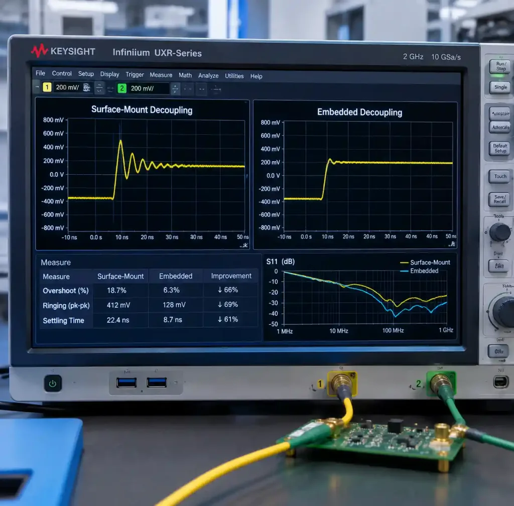
Power distribution improvement:
- Embedded decoupling capacitors closer to power pins
- Lower PDN (Power Distribution Network) impedance
- Faster transient response: <100ps vs 500ps for SMT
Physical Advantages
Size reduction:
- Typical board area savings: 30-40% for passive-heavy designs
- Height reduction: 0.3-0.6mm per embedded component layer
- Enables thinner mobile devices and wearables
Reliability improvements:
- Components protected from mechanical shock
- No solder joint fatigue for embedded parts
- Better vibration resistance (critical for automotive)
Technical Limitations
Thermal management challenges:
- Heat trapped inside board stackup
- Active components limited to <1W dissipation per die
- Thermal vias essential but add cost
Testing and rework:
- X-ray inspection required for quality control
- No functional testing before lamination
- Zero defect tolerance—embedded failures scrap entire board
Component value limitations:
- Capacitor values limited by layer thickness
- Resistor accuracy lower than precision SMT parts
- No variable or adjustable components
Applications and Market Adoption
Current Applications
Mobile devices:
- Smartphones: decoupling caps in RF sections
- Tablets: power management embedding
- Wearables: complete passive integration
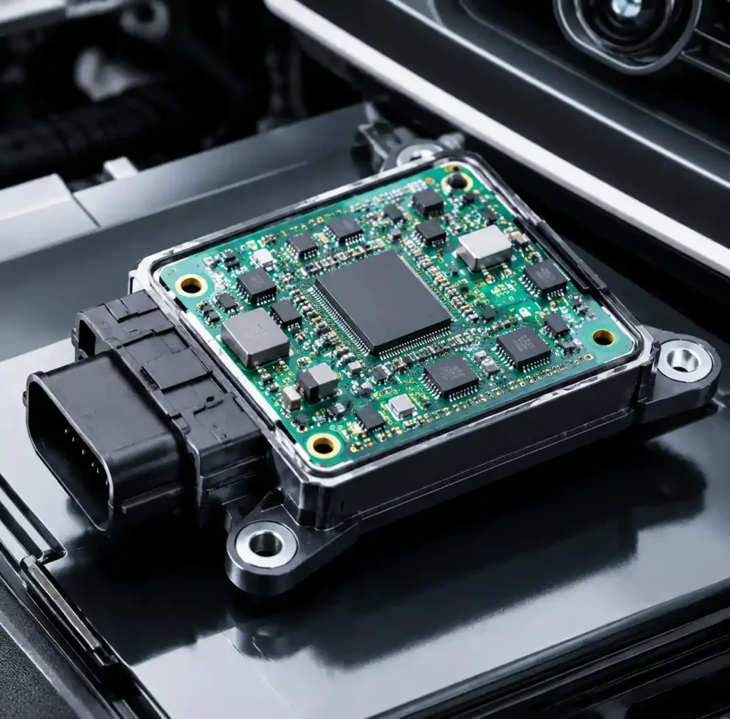
Automotive electronics:
- ADAS modules: embedded termination resistors
- Sensor modules: embedded filtering
- Requirements: AEC-Q200 qualification for embedded passives
Medical implantables:
- Pacemakers: embedded capacitors for size reduction
- Hearing aids: complete passive embedding
- Critical: biocompatibility and long-term reliability
Aerospace/Defense:
- Radar modules: embedded RF passives
- Avionics: mission-critical systems
- Qualification per IPC-6018 (Class 3)
Technology Readiness Levels
Commercially mature:
- Embedded resistors in HDI boards
- Embedded capacitors for decoupling
- Small-scale production established
Emerging technologies:
- Multi-die embedding (chiplets)
- Integrated passive devices (IPD) with active circuits
- Organic interposers with embedded components
Research phase:
- Three-dimensional component networks
- Thermal management structures
- Self-healing embedded systems
Design Guidelines and Best Practices
When incorporating embedded components in your PCB design, follow these industry-proven guidelines:
Start with passive-only designs:
- Embed decoupling capacitors first (lowest risk)
- Add resistor networks after process validation
- Defer active embedding until thermal analysis complete
Material selection:
- Use low-CTE prepregs to minimize warpage
- Match thermal expansion coefficients between core and embedded components
- Specify high-Tg materials (>170°C) for reliability
Manufacturing partner requirements:
- Verify laser drilling capability (≤100μm via diameter)
- Confirm lamination press capacity (≥400 psi)
- Require X-ray inspection equipment
- Check IPC-6018 certification for embedded technology
DFM optimization:
- Place embedded components in pairs for stackup symmetry
- Route all connections through buried/blind vias
- Add fiducial markers near embedded component zones
- Design test coupons for process validation
For complex implementations, consider starting with a hybrid approach: embed only the most critical passives while keeping other components surface-mounted. This reduces risk while capturing key benefits.
At Andwin Circuits, we manufacture HDI PCBs with embedded passive components up to 50 layers, combining embedded technology with our quick turn PCB assembly capability for prototyping and production. Our PCB manufacturing capability includes laser drilling, sequential lamination, and X-ray inspection required for embedded component production.
FAQ
Q: Can embedded components be tested before final assembly?
A: No. Embedded components are tested only after complete board fabrication through electrical testing. This requires high process control and quality assurance during embedding steps. Some manufacturers use test coupons on the panel to verify process parameters.
Q: What is the minimum order quantity for embedded component PCBs?
A: Most manufacturers require 100-500 pieces minimum due to specialized tooling and setup costs. Prototyping services may accept lower quantities at significant cost premiums (+50-100% vs standard pricing).
Q: How does embedded component technology affect repair and rework?
A: Rework is impossible for embedded components. Failed boards must be scrapped. This makes design validation and process control critical. Plan for 2-5% scrap rate in production budgets.
Q: Are there restrictions on component values for embedded passives?
A: Yes. Embedded capacitors typically limited to 10nF maximum due to layer thickness constraints. Embedded resistors range from 10Ω to 1MΩ with ±10-20% tolerance. Precision applications may require tighter process control or external trim.
Q: Which industries benefit most from embedded components?
A: Mobile devices, automotive ADAS, medical implantables, and aerospace applications show the highest adoption. Any application where size, weight, or reliability justifies the 20-40% cost premium benefits from the technology.
Q: Can I mix embedded and surface mount components in the same design?
A: Yes, and this is recommended. Embed only components where space or performance benefits justify the cost and risk. Keep standard components surface-mounted for design flexibility and easier manufacturing.
Conclusion
Embedded component technology delivers measurable benefits—30-40% size reduction, improved signal integrity, and enhanced reliability—but demands careful cost-benefit analysis. The technology makes business sense for high-volume production, space-constrained applications, and designs where electrical performance justifies the 20-50% fabrication cost premium.
Start with passive-only embedding in non-critical circuits to build experience. Establish design rules for your specific application and manufacturing partner capabilities. Calculate total cost including yield loss, testing complexity, and impossibility of rework.
The technology continues maturing. While embedded passives have reached production stability, active component embedding remains specialized. For most applications, selective embedding—placing only the most critical components internally—provides the optimal balance between cost, performance, and manufacturing risk. Focus on applications where board space translates directly to product value or where electrical performance improvements cannot be achieved through conventional design.