
PCB Underfill: Materials and Process for BGA Reliability
Thermal shock testing reveals that 60% of BGA solder joint failures in automotive electronics occur within the first 500 cycles when underfill is absent. A 2024 automotive reliability study showed underfill application extends BGA service life by 5-10× in harsh environments with temperature cycling from -40°C to +125°C.
If you want to improve BGA reliability for demanding applications, you must understand underfill material properties, application processes, curing requirements, and qualification testing. This guide explains underfill fundamentals based on production data and reliability testing from thousands of BGA assemblies.
What Is PCB Underfill?
PCB underfill is a polymer resin material dispensed beneath BGA (ball grid array) or CSP (chip scale package) components to reinforce solder joints and distribute thermomechanical stress. The material flows by capillary action into the gap between the component and PCB, then cures to form a solid protective layer.
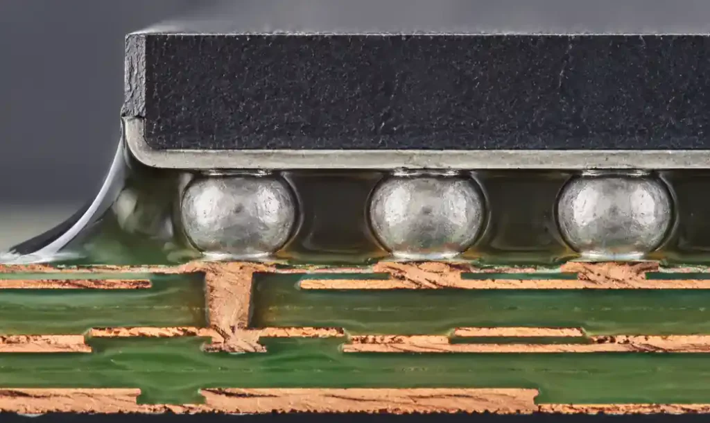
Underfill protects solder joints from failure caused by coefficient of thermal expansion (CTE) mismatch between silicon (2.6 ppm/°C), substrate (14-17 ppm/°C), and PCB (16-18 ppm/°C for FR-4). During temperature cycling, differential expansion creates shear stress at solder joints. Underfill transfers load from individual joints to the entire component body, reducing stress concentration by 70-85%.
According to IPC-7351C standards, underfill becomes necessary when reliability testing demonstrates solder joint fatigue under thermal cycling, mechanical shock, or board flexure. You should specify underfill for automotive applications per AEC-Q100 Grade 0 requirements, medical implantable devices, aerospace systems, and high-reliability industrial electronics.
Underfill Material Types and Selection
Four main underfill categories serve different manufacturing requirements and reliability objectives. Material selection depends on assembly process compatibility, cure time constraints, thermal performance needs, and cost considerations.
Capillary Flow Underfill
Capillary underfill is dispensed along component edges after reflow soldering. The low-viscosity liquid (1,000-5,000 cPs at dispensing temperature) flows under the component by capillary action, filling the 50-150μm gap between chip and PCB. Flow time ranges from 30 seconds to 3 minutes depending on component size and gap height.
| Property | Typical Value | Notes |
|---|---|---|
| Viscosity | 150-500 cPs @ 25°C | Reduces to 50-150 cPs @ 70°C |
| Flow Time | 30-180 seconds | Depends on component size |
| Cure Schedule | 150°C for 30-60 min | Or 100°C for 2-4 hours |
| Tg | 125-165°C | Higher Tg for automotive |
| CTE | 25-40 ppm/°C | Below Tg |
| Filler Loading | 50-70% | Silica particles |
Capillary underfill provides maximum reliability with CTE matched to substrate and excellent void control through proper flow. Testing shows capillary underfill achieves 2,000+ thermal cycles (-40°C to +125°C) for 15×15mm BGAs. However, the post-reflow dispensing step adds 2-5 minutes per component plus cure time.
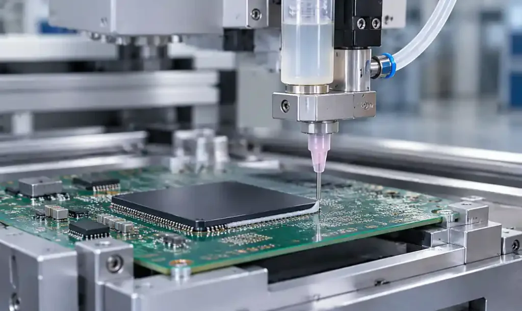
You should use capillary underfill for high-reliability applications where maximum solder joint protection justifies the process time. This includes automotive ECUs, power modules, RF transceivers, and any application requiring AEC-Q100 or MIL-STD-883 qualification.
No-Flow Underfill
No-flow underfill (also called fluxing underfill) is dispensed on the PCB pad before component placement, then cures during the standard reflow profile. The material contains flux chemistry that cleans oxide layers and promotes solder wetting while providing mechanical reinforcement.
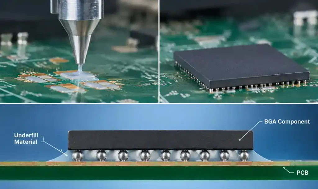
No-flow eliminates the separate underfill dispensing and cure steps, reducing assembly time by 3-5 minutes per component. SMT-compatible processing makes no-flow attractive for high-volume consumer electronics and mobile devices. However, void formation rates increase to 5-15% compared to 1-3% for capillary flow.
| Feature | Capillary Flow | No-Flow |
|---|---|---|
| Application Timing | After reflow | Before placement |
| Process Steps | Reflow + dispense + cure | Single reflow |
| Void Rate | 1-3% | 5-15% |
| Reliability | Excellent (2000+ cycles) | Good (1000-1500 cycles) |
| Cost Impact | Higher (extra step) | Lower (SMT compatible) |
| Best Use | Automotive, aerospace | Consumer, mobile |
Choose no-flow underfill when production throughput and cost reduction outweigh maximum reliability requirements. Mobile phones, tablets, and consumer IoT devices commonly use no-flow materials. Automotive and medical applications still prefer capillary flow for superior void control.
Corner Bond and Edge Bond Underfill
Corner bond (also called edge bond) applies small adhesive dots at component corners or edges rather than flowing material under the entire component. This provides basic mechanical reinforcement without hermetic sealing. Corner bonds use fast-curing adhesives (30-60 second UV cure or 5-minute thermal cure) to tack components in place.
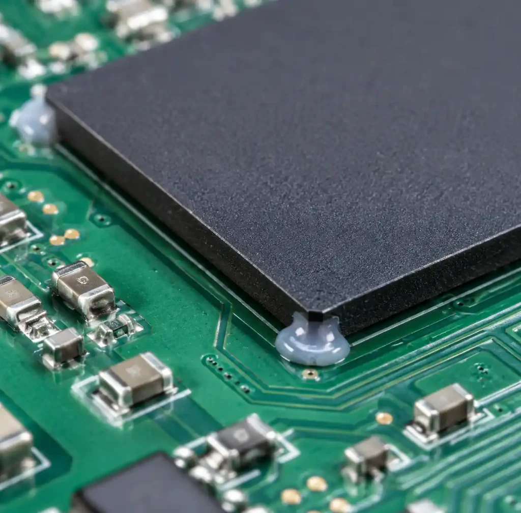
Corner bond offers minimal protection compared to full underfill but prevents component movement during handling and secondary operations. Drop test reliability improves 2-3× over non-bonded assemblies. Use corner bond for components larger than 10×10mm in portable devices subject to mechanical shock but not extreme thermal cycling.
Molded Underfill
Molded underfill uses transfer molding or compression molding to encapsulate the entire component and surrounding area. The epoxy molding compound fills gaps and provides complete environmental protection. Molded underfill achieves the highest reliability with 3,000+ thermal cycles and excellent moisture barrier properties.
However, molding adds significant cost and requires dedicated equipment. Specify molded underfill only for extreme environments including aerospace, military, and downhole oil/gas applications where hermetic sealing and maximum protection justify the expense. See MCPCB thermal management for related reliability strategies.
Underfill Material Properties and Requirements
Critical material properties determine underfill performance and compatibility with assembly processes. Understanding these parameters helps engineers specify appropriate materials for specific applications.
Glass Transition Temperature (Tg)
Tg represents the temperature where underfill transitions from rigid glassy state to soft rubbery state. Above Tg, the CTE increases dramatically (from 25-35 ppm/°C to 150-200 ppm/°C) and modulus drops by 10-100×. This degrades stress distribution and accelerates solder joint fatigue.
Select underfill Tg at least 40°C above maximum operating temperature. For automotive applications requiring -40°C to +150°C operation, specify Tg ≥ 165°C. Consumer electronics operating to +85°C can use Tg = 125-135°C materials. Testing per IPC-TM-650 Method 2.4.25 determines Tg by DSC or DMA.
Coefficient of Thermal Expansion
Underfill CTE should match substrate CTE (14-18 ppm/°C) to minimize differential expansion. CTE mismatch creates interface stresses that cause delamination. Materials with 65-75% silica filler loading achieve CTE = 25-35 ppm/°C below Tg, providing acceptable matching to organic substrates.
For ceramic substrates (CTE = 6-7 ppm/°C), use low-CTE underfills (15-25 ppm/°C) with higher filler content or specialized ceramic fillers. Measure CTE per ASTM E831 using TMA from -55°C to +200°C with heating rate 5°C/min.
Modulus and Stress Distribution
Young’s modulus affects how underfill distributes stress. Higher modulus (8-12 GPa at 25°C) provides stiffer coupling that effectively transfers load from solder joints to component body. Lower modulus (4-6 GPa) allows more compliance but provides less reinforcement.
Automotive applications benefit from high-modulus underfills that maximize stress reduction. Portable electronics may use moderate-modulus materials to tolerate board flexure without cracking. Consider modulus temperature dependence—materials maintaining >3 GPa at 125°C perform better under operating conditions.
Moisture Absorption and Outgassing
Moisture absorption (measured per JEDEC J-STD-020) should remain below 0.3 wt% after 168 hours at 85°C/85% RH. Higher moisture uptake degrades electrical insulation and causes interfacial delamination. Low molecular weight species outgas during cure, creating voids that reduce reliability.
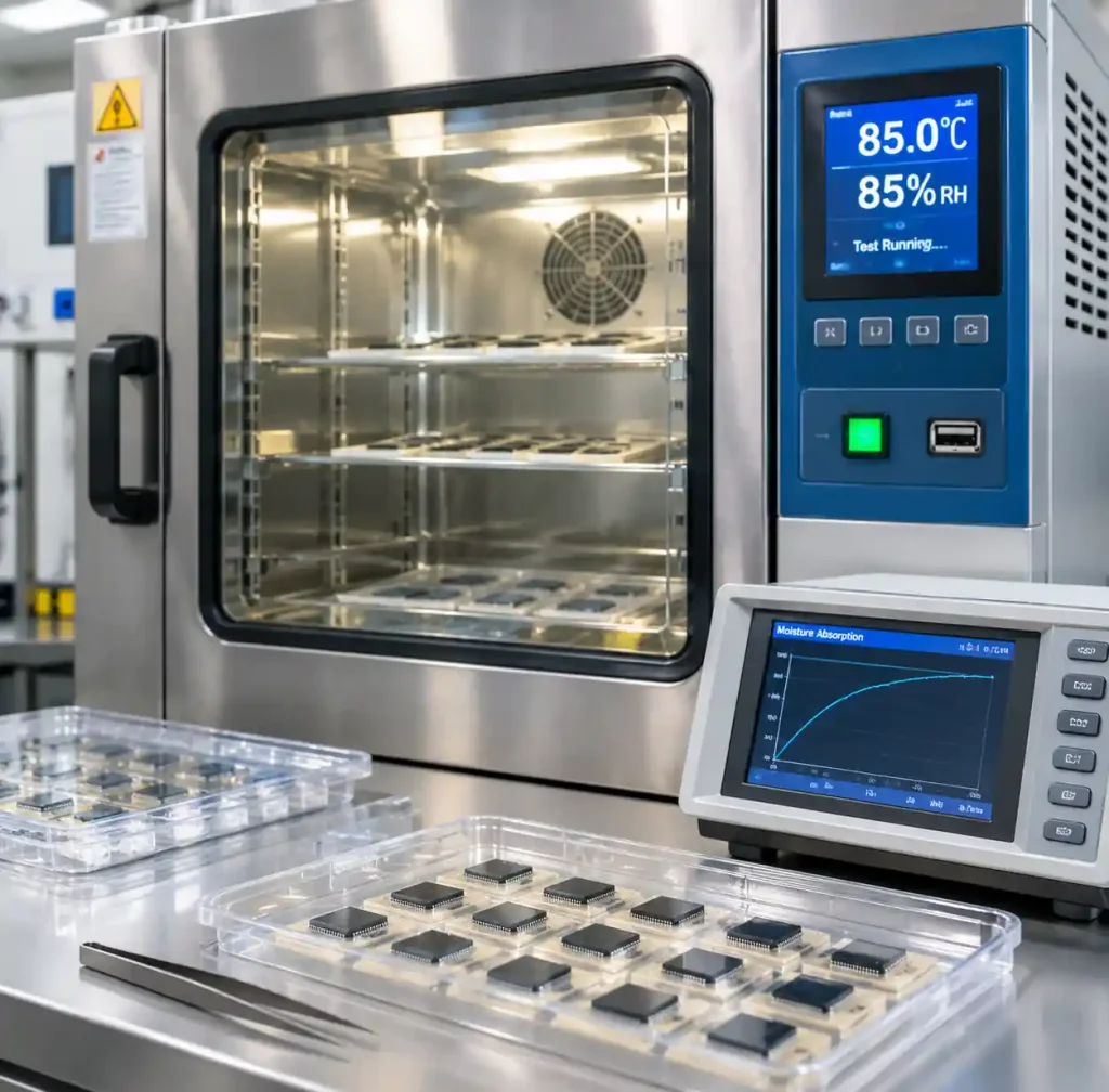
Specify underfills meeting JEDEC MSL (moisture sensitivity level) 1 classification for components requiring bake-before-use. Outgassing per ASTM E595 should show TML (total mass loss) <1% and CVCM (collected volatile condensable material) <0.1% for aerospace applications.
Underfill Dispensing and Process Control
Proper dispensing process ensures complete gap filling without voids while maintaining production throughput. Process parameters directly impact reliability—a 2025 study found 5% void content reduces thermal cycling life by 30-40%.
Capillary Flow Dispensing Parameters
Dispense along two adjacent edges for components up to 10×10mm, along all four edges for larger components. Dispensing equipment uses time-pressure or positive displacement systems. Key parameters include dispense volume (0.01-0.05mL per edge), needle diameter (18-22 gauge), dispense height (0.1-0.3mm above PCB), and temperature (substrate preheated to 60-80°C reduces viscosity and accelerates flow).
Optimize flow time by balancing viscosity, gap height, and surface energy. Typical flow rates: 5×5mm BGA fills in 30-45 seconds, 15×15mm requires 90-120 seconds, 20×20mm needs 150-180 seconds. Incomplete filling leaves unprotected solder joints susceptible to failure. Monitor with visual inspection or X-ray for internal voids.
No-Flow Process Integration
No-flow underfill requires careful reflow profile optimization. Apply 0.5-1.5mg per mm² of component area using stencil printing or jet dispensing. The material must remain tacky during component placement but not contaminate pick-and-place tooling.
| Process Parameter | Typical Range | Critical Control |
|---|---|---|
| Print Thickness | 100-200μm | Uniform coating |
| Tack Time | 10-30 minutes | Placement window |
| Reflow Peak | 245-260°C | Complete cure |
| Time Above 217°C | 60-90 seconds | Flux activation |
| Cooling Rate | 2-4°C/second | Minimize voids |
Poor profile causes voiding (too fast ramp), incomplete cure (insufficient time above Tg), or flux residue (inadequate peak temperature). Validate profiles using thermocouples on test boards with representative mass. See PCB reflow profile optimization for detailed thermal guidelines.
Cure Schedule Optimization
Underfill cure schedule affects cross-link density, residual stress, and production throughput. Typical schedules: 150°C for 30-60 minutes (fast cure), 130°C for 90 minutes (moderate), or 100°C for 2-4 hours (low-stress cure). Higher temperature cures faster but increases thermal stress due to CTE mismatch during cooldown.
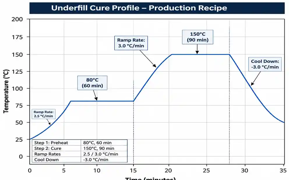
Multi-step cures provide better control: initial 80°C for 30 minutes partially cross-links material, followed by 150°C for 30 minutes to complete polymerization. This reduces residual stress while maintaining reasonable cycle time. Monitor cure with DSC to verify >95% conversion of epoxy groups.
Underfill Reliability Testing and Qualification
Rigorous reliability testing qualifies underfilled assemblies for production use. Test protocols follow IPC-9701A (thermal cycling), JESD22-B111 (board level drop test), and JEDEC JESD22-A104 (temperature cycling).
Thermal Cycling Requirements
Thermal cycling per JEDEC JESD22-A104 exposes assemblies to -40°C to +125°C cycles with 15-minute dwell times and 10-minute transition ramps. Monitor electrical continuity or perform dye-and-pry analysis at intervals. Failure criterion: >10% resistance increase or crack propagation >50% through solder joint.
Properly underfilled BGAs achieve 2,000-3,000 cycles (automotive), 1,500-2,500 cycles (industrial), or 1,000-1,500 cycles (consumer). Non-underfilled BGAs typically fail at 200-400 cycles. Testing demonstrates 5-10× life extension depending on package size and CTE mismatch severity.
Drop Test and Mechanical Shock
Board level drop testing per JESD22-B111 subjects assemblies to 1500G half-sine pulses (0.5ms duration) to simulate drop impact. Test 15 samples to 30 drops or first failure. Corner-bonded assemblies improve drop reliability 2-3× compared to non-bonded. Full underfill provides 4-6× improvement but may crack under severe impact.
Moisture and Mixed Flow Testing
Combined environmental stress includes 85°C/85% RH preconditioning followed by thermal cycling. This screens for moisture-induced delamination and interfacial adhesion loss. Assemblies must survive MSL 3 classification (168 hours moisture exposure) followed by 500+ thermal cycles without failure.
When to Specify Underfill
Underfill specification depends on application requirements, environmental conditions, and cost constraints. Not all BGAs require underfill—the decision follows reliability testing results.
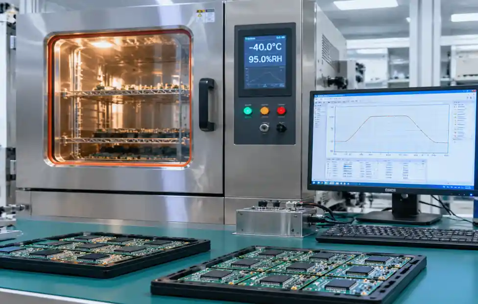
Specify underfill when qualification testing shows solder joint failures within target service life or when operating conditions exceed BGA manufacturer’s specifications. Automotive applications always require underfill per AEC-Q100 requirements. Medical implantable devices use underfill for mechanical stability and moisture protection. Aerospace and military applications specify underfill for shock and vibration resistance.
Consumer electronics may omit underfill when cost reduction outweighs reliability benefits. Mobile phones use underfill selectively for large processors (>12×12mm) but not for smaller power management ICs. IoT devices operating indoors at controlled temperature often eliminate underfill to reduce cost.
Cost analysis: capillary underfill adds $0.05-0.20 per component including material, dispense time, and cure cycle. No-flow adds $0.02-0.08 per component with minimal process impact. Balance this against field failure costs—replacing a failed automotive ECU costs $500-2,000 including labor and warranty.
Underfill Design Considerations for PCB Layout
PCB layout affects underfill flow and reliability. Provide adequate keepout zones around BGA components: minimum 3mm clearance for underfill flow on all sides, 5mm preferred for components >15×15mm. Place components >0.5mm tall within 2mm of BGA edges outside the keepout zone—these obstruct capillary flow.
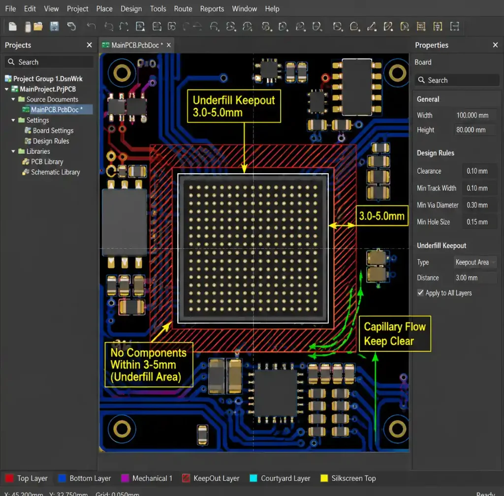
Route high-speed signals away from underfill fillet to avoid dielectric loading effects. Underfill dielectric constant (Dk = 3.5-4.2) differs from FR-4 (Dk = 4.2-4.5), creating impedance discontinuity. Maintain controlled impedance traces >2mm from component edges. See high-speed PCB design guidelines for signal integrity optimization.
Thermal vias under BGA thermal pads must extend beyond underfill region to function effectively. Place via arrays with 0.8-1.2mm pitch and route to internal ground planes. Underfill improves thermal performance 15-25% by filling air gaps but remains 10× less conductive than copper. Combine underfill with thermal via design for power devices.
Common Underfill Defects and Prevention
Voids represent the most common underfill defect, occurring in 3-12% of components depending on process control. Voids larger than 15% of underfill area significantly degrade reliability. Causes include trapped air during flow, moisture outgassing, or volatile components. Prevent voids through substrate preheating (70-80°C), slow dispense rates, vacuum-assisted flow for large components, and proper material selection (low volatiles).
Fillet non-uniformity creates stress concentration points. Ensure complete fillet around all component edges, 45-degree fillet angle, and height 30-50% of component thickness. Incomplete filling leaves solder joints unprotected. Monitor with visual inspection under magnification or automated optical inspection (AOI).
Delamination between underfill and PCB or component occurs due to poor surface preparation, moisture contamination, or CTE mismatch. Prevent through flux residue removal, plasma surface treatment, material selection with good adhesion, and proper cure schedule. Acoustic microscopy detects delamination non-destructively during qualification testing.
Frequently Asked Questions
What is the difference between underfill and encapsulant?
Underfill specifically fills the gap under BGA or flip-chip components to protect solder joints, while encapsulant coats the entire component and surrounding area for environmental protection. Underfill flows by capillary action and requires low viscosity (150-500 cPs). Encapsulant is applied by dam-and-fill or molding with higher viscosity (5,000-50,000 cPs).
Can underfill be reworked?
Capillary underfill can be reworked but requires heating to 200-250°C to soften the polymer before component removal. Specialized rework tools apply focused heat while protecting surrounding components. Rework success rate drops to 60-80% compared to 95%+ for non-underfilled BGAs. See BGA rework procedures for process details.
How does underfill affect PCB assembly cost?
Capillary underfill adds $0.05-0.20 per component including material ($0.02-0.05), dispense time (30-90 seconds), and cure cycle (pro-rated). No-flow underfill adds $0.02-0.08 per component with SMT-compatible processing. Cost justification depends on failure rate reduction and field repair costs.
What temperature rating should underfill have?
Select underfill Tg at least 40°C above maximum operating temperature. Automotive Grade 0 (-40°C to +150°C) requires Tg ≥ 165°C. Industrial applications (+85°C max) use Tg ≥ 130°C. Consumer electronics (+70°C typical) can use Tg ≥ 110°C. Higher Tg provides better reliability margin.
Does underfill improve thermal performance?
Underfill provides 15-25% thermal improvement by filling air gaps (thermal conductivity 0.6-1.0 W/mK vs 0.026 W/mK for air). However, underfill remains 10-20× less conductive than thermal interface materials. For power devices requiring maximum thermal performance, combine underfill with proper via design and consider metal core PCB construction.
Conclusion
Underfill technology significantly extends BGA solder joint reliability in harsh environments. Selecting appropriate underfill materials, optimizing dispensing processes, and qualifying assemblies through rigorous testing ensures product success. Capillary flow provides maximum reliability for automotive and aerospace applications. No-flow reduces cost for consumer electronics while maintaining acceptable performance.
If you need PCB assembly services with underfill application for automotive, medical, industrial, or consumer electronics, Andwin Circuits provides complete turnkey solutions with advanced BGA assembly capabilities. Our facility uses automated underfill dispensing systems and maintains ISO 9001, IATF 16949, and IPC-A-610 Class 3 certifications. We have successfully delivered underfilled assemblies for automotive ADAS systems, medical monitoring devices, and high-reliability industrial controllers.
Contact us today for custom PCB assembly solutions with underfill expertise, reliability testing support, and competitive factory-direct pricing.
Sources: