
3D Printed Electronics: Additive Manufacturing for PCB Prototyping
Additive manufacturing for PCBs reduces material waste by 50-90% compared to traditional subtractive processes and eliminates tooling costs for prototypes. According to recent industry analysis, 3D printed electronics technology has advanced beyond laboratory experiments into practical applications for wearable sensors, flexible antennas, and rapid prototyping where traditional manufacturing faces limitations.
In today’s article, we will examine additive manufacturing technologies for PCB prototyping, including conductive ink jetting, aerosol jet printing, and laser direct structuring. This guide will help hardware engineers and product designers understand when 3D printed electronics offer advantages over traditional PCB fabrication for prototype development and specialized applications.
What is 3D Printed Electronics?
3D printed electronics refers to additive manufacturing processes that create functional circuit boards by depositing conductive materials layer by layer rather than removing copper from a substrate. This approach uses conductive inks, silver nanoparticles, or copper materials to build circuits directly on substrates through inkjet printing, aerosol deposition, or hybrid additive-subtractive methods.
Unlike traditional PCB manufacturing that etches unwanted copper from a laminated board, additive PCB processes deposit conductive traces only where required. You can create three-dimensional circuit geometries, embed components during printing, and prototype functional boards in hours rather than days or weeks required for conventional fabrication.
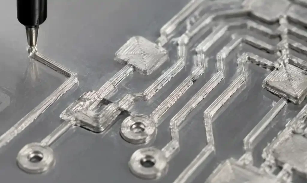
The technology enables rapid design iteration for IoT devices, wearable electronics, and research applications where low-volume production and geometric flexibility outweigh the higher conductivity of traditional copper traces. Aerosol jet printing achieves trace widths down to 10 micrometers with silver ink conductivity reaching 10-40% of bulk copper after sintering.
Additive Manufacturing Technologies for PCB
Conductive Ink Jetting
Conductive ink jetting uses piezoelectric or thermal printheads to deposit silver or copper nanoparticle inks onto substrates. This process achieves trace widths of 50-200 micrometers with conductivity values between 20-60% of bulk copper depending on ink formulation and curing method.
The inkjet approach works best for prototyping simple circuits with moderate current requirements below 1A per trace. You should specify thermal curing at 150-250°C or UV sintering to achieve optimal conductivity. Component assembly follows standard SMT processes after ink curing completes.
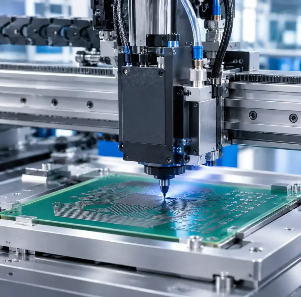
Desktop inkjet systems cost $5,000-50,000 and produce prototype boards in 2-4 hours including curing time. Material costs range from $200-800 per liter of conductive ink with typical consumption of 5-15 ml per 100 cm² board area.
Aerosol Jet Printing
Aerosol jet printing atomizes conductive inks into microdroplets and focuses them through a pneumatic stream onto the substrate. This technology achieves 10-50 micrometer trace resolution with excellent edge definition and layer thickness control between 0.5-5 micrometers.
The process deposits silver inks with conductivity reaching 40% of bulk copper after thermal sintering at 200-300°C. You can print conformal circuits on curved 3D surfaces, integrate passive components, and create multilayer structures with dielectric printing between conductor layers. Aerosol jet printing handles complex geometries that traditional PCB cannot achieve, including circuits on cylindrical surfaces, inside housings, and on flexible substrates.
Industrial aerosol jet systems cost $150,000-500,000 with print speeds of 100-500 mm/s and positioning accuracy within 10 micrometers. Applications include antenna fabrication, sensor integration, and RF circuits for wireless devices operating between 1-10 GHz.
Laser Direct Structuring (LDS)
Laser direct structuring activates thermoplastic substrates doped with laser-sensitive additives, creating nucleation sites for subsequent metallization. A laser traces the circuit pattern, and chemical plating deposits copper onto activated areas with conductivity approaching bulk copper performance.
This hybrid process combines injection molding with circuit fabrication in a single component. You can specify complex 3D circuit geometries integrated directly into device housings, eliminating separate PCB mounting and reducing assembly steps by 40-60% for automotive sensors, smartphone antennas, and medical devices.
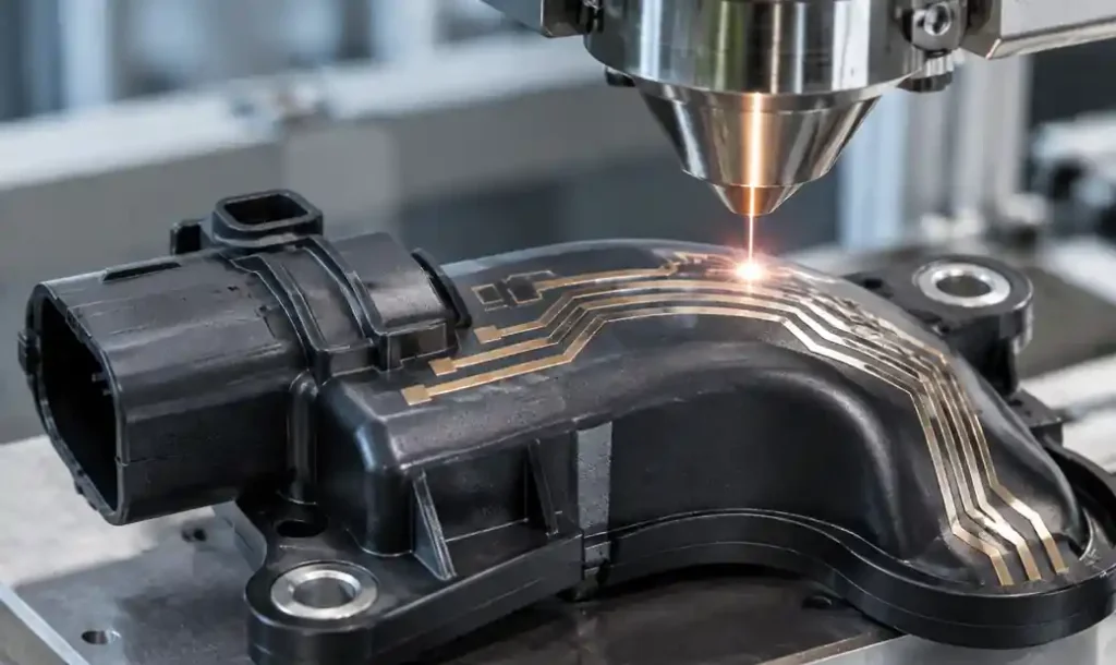
LDS achieves trace widths down to 100 micrometers with copper thickness of 5-15 micrometers after plating. The process requires specialized thermoplastic materials but delivers excellent electrical performance for high-frequency applications above 2 GHz. Tooling costs range from $10,000-100,000 for injection molds with per-unit costs economical above 1,000 units.
3D Printed PCB vs Traditional PCB Manufacturing
| Parameter | 3D Printed PCB | Traditional PCB |
|---|---|---|
| Trace Conductivity | 10-60% of copper | 100% copper (17-210 μm) |
| Minimum Trace Width | 10-200 μm | 75-150 μm (standard) |
| Prototype Lead Time | 2-8 hours | 5-15 days |
| Setup Cost | $0 (digital) | $100-500 (tooling) |
| Material Waste | 5-10% | 40-70% |
| 3D Geometry | Full 3D circuits | Planar only |
| Layer Count | 1-4 layers | 2-50+ layers |
| Current Capacity | 0.1-2A per trace | 1-100+ A per trace |
| Cost per Unit (10 pcs) | $50-200 | $5-30 |
| Cost per Unit (1000 pcs) | $30-150 | $1-5 |
Choose 3D printed electronics when you need rapid prototype iteration, complex 3D geometries, or low-volume production below 100 units where tooling costs dominate traditional manufacturing. Traditional PCB remains superior for production volumes above 500 units, high current applications, and designs requiring more than 4 layers.
Applications for 3D Printed Electronics
Rapid Prototyping and Design Iteration
Additive PCB manufacturing reduces prototype lead time from 5-15 days to 2-8 hours by eliminating tooling and offshore fabrication. You can test design concepts, verify circuit functionality, and iterate layouts within a single workday rather than waiting for manufacturer turnaround.
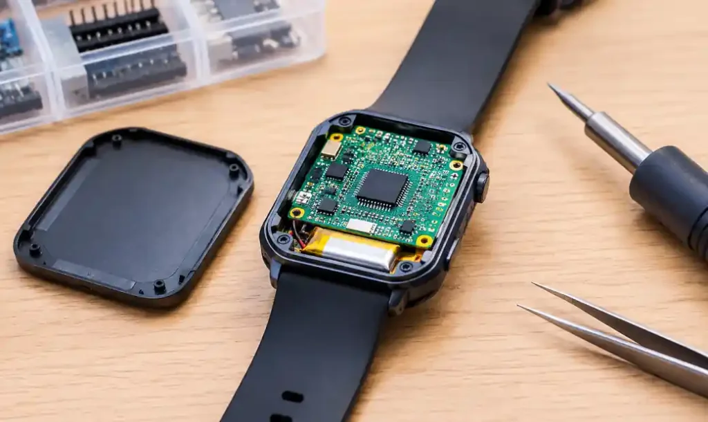
This speed advantage benefits IoT device development, wearable electronics, and research applications where design exploration requires multiple prototype cycles. Desktop systems enable in-house prototyping with material costs of $10-50 per board for simple circuits under 100 cm² area.
Wearable and Flexible Electronics
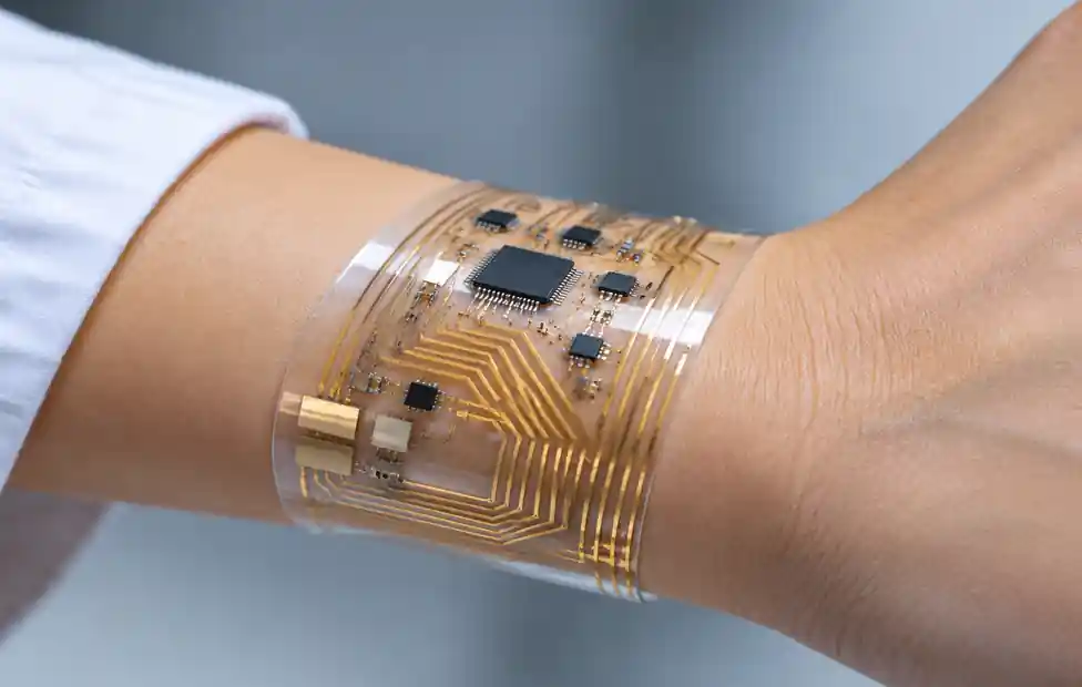
3D printed electronics enable conformal circuits on textiles, flexible substrates, and curved surfaces for wearable sensors, smart clothing, and medical monitoring devices. You can print silver ink traces on polyimide, PET, or fabric substrates with bend radii down to 1-5 mm for dynamic flexing applications.
Aerosol jet printing creates stretchable interconnects by depositing serpentine traces that accommodate up to 30% substrate elongation. Applications include ECG sensors, motion tracking devices, and temperature monitoring patches that conform to body contours.
Molded Interconnect Devices (MID)
Laser direct structuring integrates circuits directly into injection-molded plastic housings for automotive sensors, smartphone antennas, and medical device assemblies. This approach reduces part count by 50-70% compared to separate PCB mounting and improves reliability by eliminating connectors and solder joints.
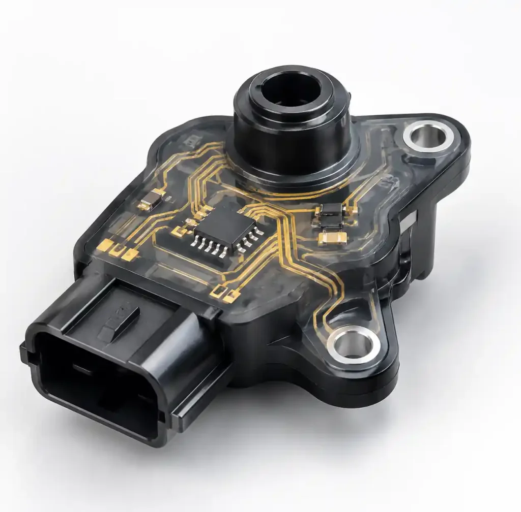
You can specify 3D antenna geometries optimized for specific frequencies, embed circuits inside structural components, and create waterproof assemblies without additional sealing. LDS MID components handle operating temperatures from -40°C to +120°C with thermal cycling performance meeting automotive AEC-Q200 requirements.
Antenna and RF Circuits
Additive manufacturing creates conformal antennas and RF circuits on curved surfaces for IoT devices, drones, and aerospace applications. Aerosol jet printing deposits silver ink traces with controlled impedance for 2.4 GHz Wi-Fi, 5-6 GHz WLAN, and sub-GHz LoRa antennas.
You can optimize antenna geometry for specific radiation patterns without the planar constraints of traditional PCB. Three-dimensional antenna structures improve gain by 2-4 dB compared to equivalent flat designs while reducing board space by integrating antennas into device housings or curved panels.
Design Considerations for 3D Printed PCB
Conductivity and Current Limits
3D printed conductive traces achieve 10-60% of bulk copper conductivity depending on ink formulation and curing method. Silver nanoparticle inks reach 40-60% after thermal sintering at 250-300°C, while lower-temperature UV-cured inks provide 10-30% conductivity.
You should limit current to 0.5-2A per trace for typical printed conductors with 100-200 micrometer width and 5-10 micrometer thickness. Calculate voltage drop using measured trace resistance rather than copper values – expect 5-10× higher resistance than equivalent copper traces. Parallel traces or increased width compensates for lower conductivity in power distribution paths.
Trace Resolution and Spacing
Aerosol jet printing achieves minimum trace width of 10 micrometers with spacing down to 20 micrometers for fine-pitch applications. Inkjet systems typically deliver 50-150 micrometer traces with 100-200 micrometer spacing depending on ink viscosity and substrate surface energy.
Design rules for 3D printed PCB should specify minimum features 2-3× larger than equipment capability to ensure manufacturability. Allow 200-500 micrometer clearance around SMT component pads for assembly tolerance. Via formation requires through-hole drilling or laser ablation followed by conductive ink filling with multiple print passes.
Layer Stackup and Dielectric
Multilayer 3D printed circuits require dielectric printing between conductor layers using UV-curable polymers or screen-printed insulators. Dielectric thickness of 25-100 micrometers provides adequate interlayer isolation for signal routing below 1 GHz.
You can achieve 2-4 layer structures with registration accuracy within 50-100 micrometers between layers. Impedance control remains challenging due to dielectric constant variations in printed materials – expect ±15-25% tolerance compared to ±10% for traditional PCB laminates. High-frequency designs above 2 GHz should use LDS or traditional PCB for controlled impedance routing.
Cost Analysis: 3D Printed vs Traditional PCB
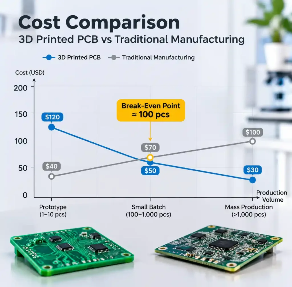
| Production Volume | 3D Printed PCB Cost | Traditional PCB Cost | Break-Even Analysis |
|---|---|---|---|
| 1-10 units | $50-200/board | $150-500/batch + $20/board | 3D printing cheaper |
| 50-100 units | $30-100/board | $200-500/batch + $8/board | Approximately equal |
| 500-1000 units | $25-80/board | $300-800/batch + $2-5/board | Traditional cheaper |
| 5000+ units | $20-60/board | $500-1500/batch + $0.50-2/board | Traditional 90% cheaper |
Choose 3D printed electronics for prototype quantities below 50 units where traditional tooling costs dominate total expenses. Consider traditional PCB manufacturing for production volumes above 500 units where per-unit costs and superior electrical performance justify tooling investment.
Hybrid approaches combine traditional PCB for complex multilayer circuits with 3D printed antennas or sensors for geometric flexibility. You can specify conventional FR4 boards for power and signal processing with aerosol jet printed conformal antennas integrated onto device housings.
Limitations of 3D Printed Electronics
Conductivity and Electrical Performance
Conductive inks achieve only 10-60% of bulk copper conductivity, limiting current capacity and increasing voltage drop in power distribution networks. Resistance values of 10-100 mΩ per square for printed silver traces compare unfavorably to 0.5-5 mΩ per square for copper, requiring wider traces or parallel paths for equivalent performance.
High-frequency applications above 5 GHz suffer from increased skin effect losses in printed conductors with surface roughness of 1-5 micrometers compared to 0.2-1 micrometer for electrodeposited copper. Signal integrity analysis should account for 3-5× higher losses in printed traces when designing RF circuits or high-speed digital interfaces.
Resolution and Layer Count
Current 3D printed PCB technology limits practical designs to 4 layers with trace/space capabilities of 50-100 micrometers for reliable manufacturing. This restricts component density and routing complexity compared to HDI PCB achieving 3 mil (75 micrometer) traces across 20+ layers.
Via formation requires multiple process steps with reliability concerns for high aspect ratio connections. Microvia technology common in traditional HDI remains difficult to replicate with printed electronics, limiting applications to moderate-density circuits below 500 components per board.
Cost at Production Volumes
Material costs of $200-800 per liter for conductive inks and print times of 10-30 minutes per board make 3D printed electronics uneconomical for volumes above 1000 units. Traditional PCB achieves $0.50-5 per board in production quantities with superior electrical performance and reliability.
Equipment costs of $150,000-500,000 for industrial aerosol jet systems require production volumes of 5,000-20,000 boards annually to justify investment compared to outsourced traditional manufacturing. Desktop inkjet systems at $5,000-50,000 suit research and low-volume prototyping but cannot match production efficiency of conventional PCB fabrication.
Future Developments in 3D Printed PCB
Materials Innovation
Copper nanoparticle inks under development target 70-90% bulk copper conductivity with sintering temperatures below 200°C for temperature-sensitive substrates. Graphene and carbon nanotube inks offer 1-10 S/cm conductivity for flexible electronics applications requiring extreme bend cycles above 10,000 cycles.
Printed dielectrics with low loss tangent below 0.01 at 5 GHz will enable controlled impedance structures for high-frequency applications. Multi-material printing systems will deposit conductors, dielectrics, and semiconductors in single-pass processes, reducing assembly steps by 60-80% for integrated electronics.
Process Improvements
Machine learning algorithms optimize print parameters in real-time, reducing defect rates from 10-20% to below 5% for production-quality boards. Hybrid systems combine aerosol jet printing for fine features with screen printing for area fills, achieving 50% faster throughput while maintaining 10 micrometer resolution where needed.
In-situ monitoring with machine vision and electrical testing validates conductivity during printing, enabling immediate correction rather than discovering failures after curing. These improvements will reduce printed electronics costs by 40-60% over the next 3-5 years while improving reliability to match traditional PCB standards.
Frequently Asked Questions
Can 3D printed electronics replace traditional PCB manufacturing?
No, 3D printed electronics currently cannot replace traditional PCB for most applications due to lower conductivity (10-60% of copper), limited layer count (1-4 layers), and higher costs above 500 units. The technology serves specialized applications requiring rapid prototyping, 3D geometries, or ultra-low volume production where tooling costs dominate traditional manufacturing. Traditional PCB remains superior for production volumes, high current capacity, and multilayer designs above 4 layers.
What is the minimum trace width achievable with 3D printed PCB?
Aerosol jet printing achieves minimum trace widths of 10-20 micrometers under controlled conditions, while inkjet systems typically deliver 50-100 micrometer traces. Practical design rules should specify 50-100 micrometer minimum width for aerosol jet and 100-200 micrometer for inkjet to ensure reliable manufacturing. These capabilities compare to 75-150 micrometer (3-6 mil) standard traces in traditional PCB or 50 micrometer (2 mil) for advanced HDI manufacturing.
How long does it take to 3D print a PCB prototype?
Desktop inkjet systems produce simple single-layer boards in 2-4 hours including ink curing time for 100-200 cm² area. Aerosol jet printing requires 4-8 hours for multilayer designs with dielectric layers and multiple curing steps. Traditional quick-turn PCB services deliver finished boards in 24-48 hours for standard specifications or 5-7 days for complex HDI stackups. The time advantage of 3D printing matters most for in-house prototyping with multiple design iterations within a single day.
What conductive materials are used for 3D printed electronics?
Silver nanoparticle inks provide the highest conductivity (40-60% of bulk copper) after thermal sintering at 200-300°C with costs of $300-600 per liter. Copper nanoparticle inks offer lower material costs ($200-400 per liter) but require inert atmosphere processing to prevent oxidation during sintering. Carbon-based inks (graphene, carbon nanotubes) achieve 1-10 S/cm conductivity for flexible electronics at $500-1200 per liter, suitable for low-current applications like sensors and antennas.
Is 3D printed PCB suitable for high-frequency RF applications?
Limited suitability exists for RF applications below 5 GHz using aerosol jet printed silver inks with optimized trace geometry. Surface roughness of 1-5 micrometers in printed conductors increases skin effect losses at high frequencies compared to 0.2-1 micrometer for electrodeposited copper. Laser direct structuring (LDS) with electroplated copper performs better for 5-10 GHz applications approaching traditional PCB performance. For frequencies above 10 GHz or controlled impedance below ±5%, traditional PCB with Rogers or Taconic laminates remains the preferred solution.
What are the environmental benefits of 3D printed PCB?
Additive manufacturing reduces material waste by 50-90% compared to subtractive PCB etching that removes 40-70% of the copper laminate as waste. The process eliminates chemical etching with hazardous etchants (ferric chloride, ammonium persulfate) and reduces water consumption by 60-80% per board. Energy consumption for desktop 3D printing averages 0.2-0.5 kWh per board versus 0.8-2 kWh for traditional manufacturing including drilling, plating, and etching steps. However, conductive ink production requires significant energy and the inks themselves contain silver nanoparticles requiring proper disposal.
Conclusion
3D printed electronics using conductive ink jetting, aerosol jet printing, and laser direct structuring enables rapid PCB prototyping in 2-8 hours with 50-90% material waste reduction compared to traditional manufacturing. These additive technologies suit low-volume production below 100 units, design iteration requiring multiple prototype cycles, and specialized applications needing 3D circuit geometries or conformal integration.
Current limitations include 10-60% copper conductivity restricting current capacity to 0.5-2A per trace, practical designs limited to 4 layers, and costs 5-10× higher than traditional PCB above 500 unit volumes. The technology serves niche applications in wearable electronics, IoT prototyping, and molded interconnect devices where geometric flexibility and rapid turnaround justify tradeoffs in electrical performance and production cost.
If you need high-quality PCB prototyping or production services for your electronic device project, Andwin Circuits offers advanced manufacturing capabilities up to 50 layers with fast delivery in 7 days. Our facility handles traditional PCB fabrication, HDI technology, rigid-flex circuits, and quick-turn assembly services with ISO 9001 and IATF 16949 certification ensuring reliable quality for automotive, medical, telecommunications, and IoT applications worldwide.
Contact us today for custom PCB manufacturing solutions, technical specifications, and competitive factory-direct pricing for your prototype or production requirements.