
PCB Assembly Lead Time: What Affects Manufacturing Speed?
PCB assembly lead time ranges from 8 hours for expedited prototypes to 6 weeks for complex production runs, with typical projects requiring 10-15 days. Studies show that 40% of electronics product delays stem from inaccurate lead time estimates and component availability issues.
This guide breaks down PCB assembly lead time into its core phases and identifies what slows each stage, showing you how to reduce total time-to-market through smarter planning and design-for-manufacturing practices.
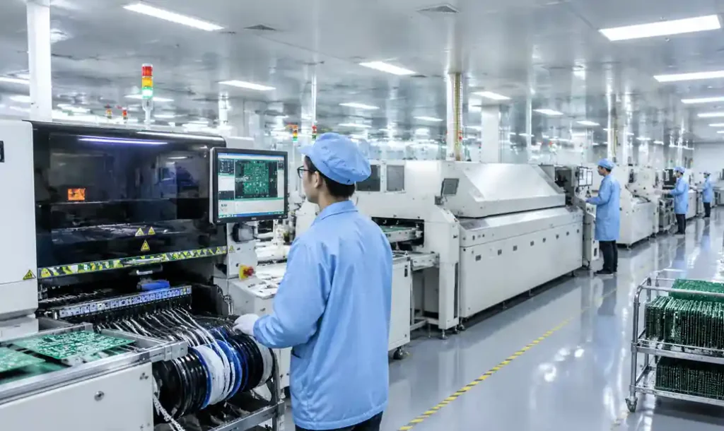
What Is PCB Assembly Lead Time?
PCB assembly lead time is the duration from order confirmation to finished, tested boards ready for integration. This timeline includes four sequential phases: PCB fabrication (bare board manufacturing), component procurement (sourcing and inspection), assembly operations (SMT/through-hole placement), and final testing (AOI, X-ray, functional test).
Standard lead time for a 4-6 layer board with common components runs 10-15 days. Quick-turn services compress this to 3-7 days by running fabrication and sourcing in parallel. High-layer-count boards (10+ layers), specialty materials, or hard-to-source components extend timelines to 3-6 weeks.
Lead time calculation starts after design files pass DFM review and engineering questions are resolved. A design with spacing violations adds 1-3 days for clarification before fabrication begins.
PCB Fabrication Phase: Bare Board Manufacturing
Layer Count and Stackup Complexity
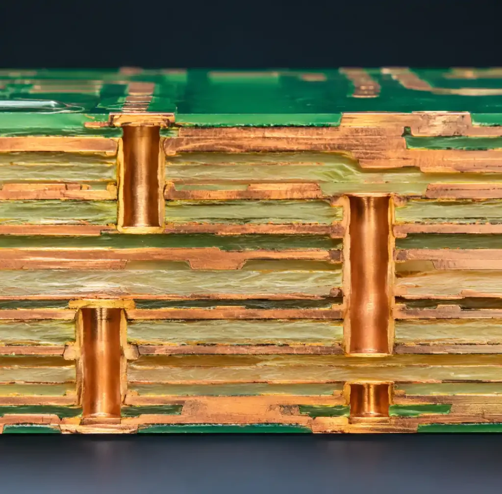
Fabrication time scales directly with layer count. A 2-layer board completes in 24-48 hours with only two copper etching cycles and one lamination press. An 8-layer board needs four copper layers per side, multiple lamination stages, and extended drill/plating cycles, pushing fabrication to 7-10 days.
HDI boards with blind and buried vias add 2-4 days due to sequential build-up lamination and laser drilling operations. Each microvia layer requires separate imaging, drilling, and plating. Standard through-hole boards finish faster.
Thick boards (2.4mm+) or heavy copper designs (3oz+) require longer press times to prevent warpage. Andwin Circuits manufactures boards up to 50 layers with controlled impedance, typically delivered in 7-15 days.
Material Selection and Availability
FR-4 laminates ship immediately from stock, adding zero delay. High-frequency materials (Rogers RO4350B) require 3-7 days procurement because manufacturers stock limited quantities. Ceramic substrates for extreme thermal applications add 2-3 weeks.
Surface finish selection impacts throughput. HASL completes in 30 minutes per panel. ENIG requires 4-6 hours for nickel plating and gold deposition. OSP applies in 15 minutes but offers shorter shelf life.
| Board Type | Layer Count | Typical Fabrication | Quick Turn |
|---|---|---|---|
| Standard PCB | 2-4 layers | 3-5 days | 24-48 hours |
| Multilayer PCB | 6-8 layers | 7-10 days | 3-5 days |
| High-Layer PCB | 10-20 layers | 10-15 days | 5-7 days |
| HDI PCB | 4-10 layers | 10-14 days | 5-7 days |
| Rigid-Flex PCB | 4-8 layers | 12-18 days | 7-10 days |
Component Procurement: The Hidden Bottleneck
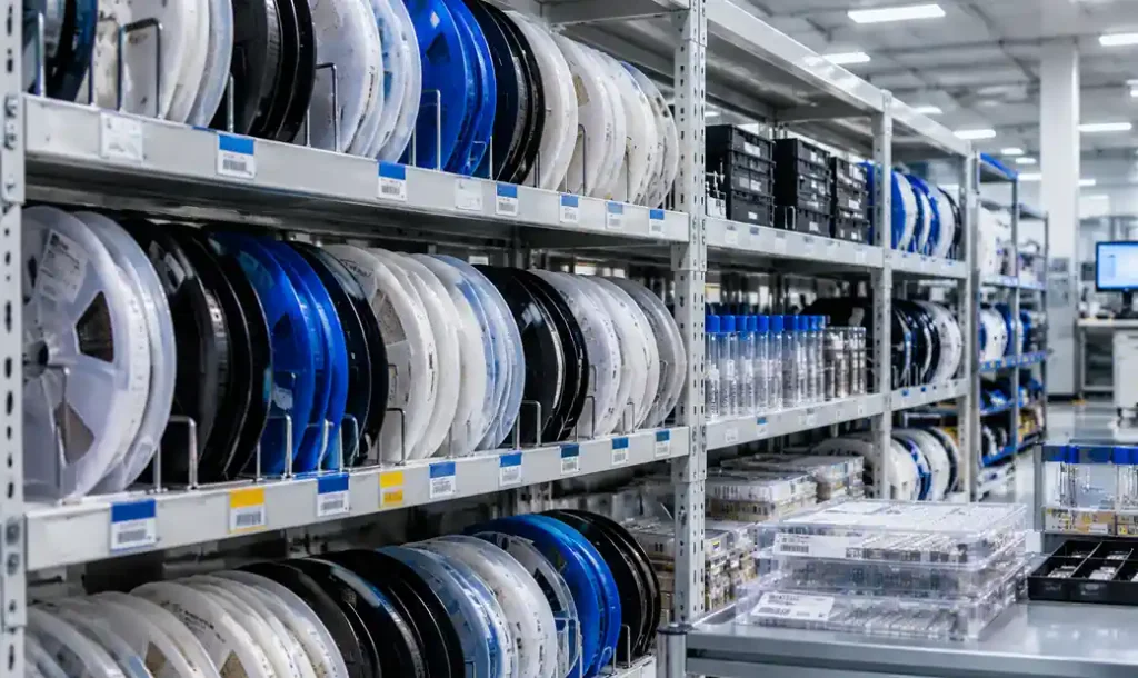
Component sourcing accounts for 40-60% of total assembly delays in 2025-2026. Common passives and jellybean ICs ship from distributor stock in 1-2 days. Specialized microcontrollers, FPGAs, and power management ICs may require 8-16 weeks factory lead time during allocation periods.
Consigned assembly (you provide components) eliminates procurement delays but shifts sourcing risk to your team. Turnkey assembly (manufacturer sources components) adds 3-7 days for standard BOMs and 2-4 weeks for boards with allocated parts.
Authorized distributors guarantee authentic parts with traceable date codes. For aerospace, medical, and automotive applications requiring full traceability, stick to authorized channels even if procurement extends by 1-2 weeks.
Design with commonly stocked components to minimize delays. Run BOM checks against distributor inventory during design to identify long-lead parts early. Avoid single-source components unless performance mandates it. Accept wider tolerance ranges on passives when performance allows—a 1% resistor with 8-week lead time may be unnecessary when 5% tolerance performs identically.
Assembly Operations: SMT and Through-Hole
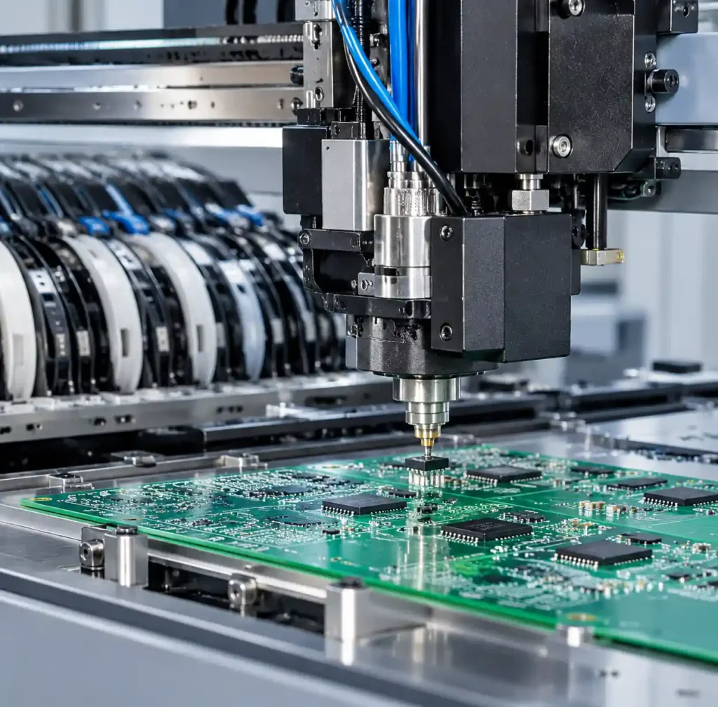
SMT placement rate averages 15,000-30,000 components per hour, but setup time dominates small-batch runs. A board with 200 unique component types requires 2-4 hours for feeder setup and kitting before production begins. Panels run through reflow at 3-5 minutes per panel.
Fine-pitch components (0.4mm pitch BGAs, 01005 passives) reduce placement speed by 40-60% due to vision alignment cycles. QFNs with exposed thermal pads require selective solder paste printing and X-ray inspection after reflow, adding 30-60 minutes per panel.
Through-hole components extend assembly time. Wave soldering adds 1-2 hours. Hand soldering for mixed-technology boards consumes 5-15 minutes per board. Andwin Circuits offers both SMT and mixed-technology assembly with IPC-A-610 Class 3 workmanship.
First-time orders require stencil fabrication (2-3 days) and test fixture design if functional testing applies (3-5 days). Repeat orders with existing stencils eliminate this setup phase. Panel depaneling method impacts throughput—V-score completes in seconds, tab routing requires 2-5 minutes per panel.
Testing and Quality Control
AOI runs at 30-60 seconds per panel and catches 95%+ of placement defects. X-ray inspection for BGA packages adds 2-3 minutes per board to verify hidden solder joints.
Flying probe testing provides 85-90% net coverage without custom fixtures, ideal for prototypes. Test time scales with net count: 200 nets test in 3-5 minutes, 1000 nets require 15-20 minutes. ICT with bed-of-nails fixtures achieves 98%+ coverage but requires custom fixture design (3-7 days) and $500-$2000 NRE cost.
| Test Method | Coverage | Test Time | Fixture Cost | Best For |
|---|---|---|---|---|
| AOI | 95% | 30-60s | None | All volumes |
| X-ray | 100% | 2-3 min | None | BGA/QFN |
| Flying Probe | 85-90% | 3-20 min | None | <500 units |
| ICT | 98%+ | 1-3 min | $500-$2000 | >500 units |
| Functional | 100% | 30s-15 min | $1000-$5000 | Mission-critical |
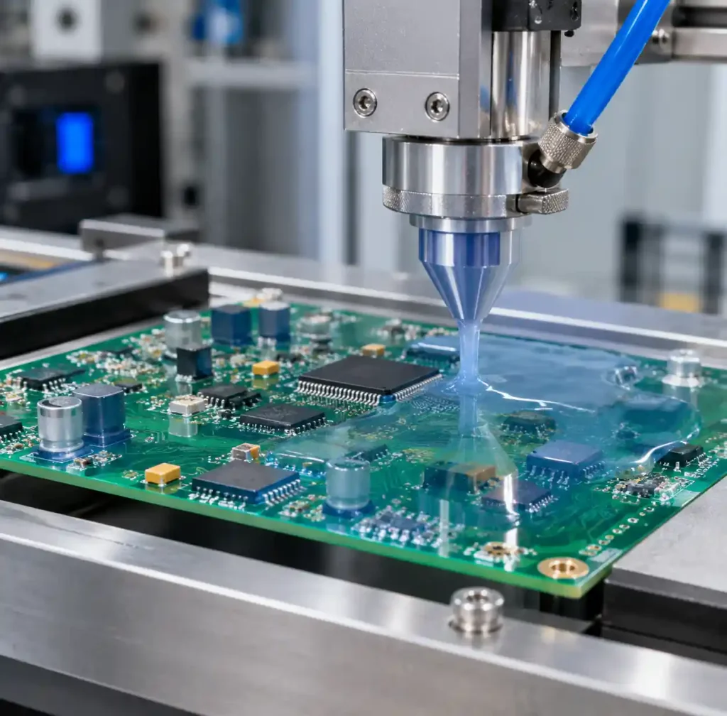
First-pass yield averages 92-98% for standard SMT assemblies when DFM rules are followed. Boards with design violations drop to 70-85% yield, triggering rework cycles that add 1-3 days. BGA rework consumes 20-30 minutes per device. Conformal coating adds 1-2 days for application and cure time.
Lead Time Reduction Strategies
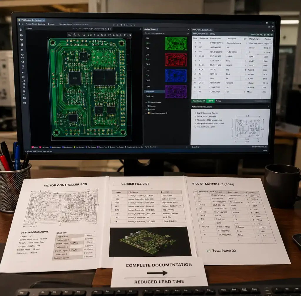
DFM-optimized designs reduce assembly time by 25-40% compared to designs with violations. Avoid components smaller than 0201 unless miniaturization demands it. Use standard land patterns from IPC-7351 to ensure first-pass placement accuracy.
Minimize unique component types to reduce feeder setup time. A board with 50 unique parts sets up faster than a board with 150 unique parts even if total component count is identical. Provide complete documentation: Gerbers, drill files, BOM with manufacturer part numbers, assembly drawings, and special process requirements.
Quick-turn services run fabrication and component procurement in parallel. Expedite fees range from 30% premium for 50% time reduction to 100%+ premium for 24-hour turnaround. Reserve expedites for true schedule emergencies.
Partner with manufacturers offering turnkey kitting services that maintain buffer stock of common components. This eliminates distributor shipping time for 60-80% of your BOM. Andwin Circuits stocks standard components and offers 7-day turnkey assembly for boards up to 10 layers.
Submit Gerbers 2-3 business days before you need fabrication to start. This allows DFM review and component availability checks. Respond to engineering questions within 4 business hours to keep your order on schedule.
Order Quantity and Production Volume
Small-batch orders (10-50 units) spend proportionally more time in setup than production. A 20-board build may take 6 hours: 3 hours setup, 1.5 hours placement, 0.5 hours reflow, 1 hour testing. Doubling to 40 units adds only 2 hours because setup is complete.
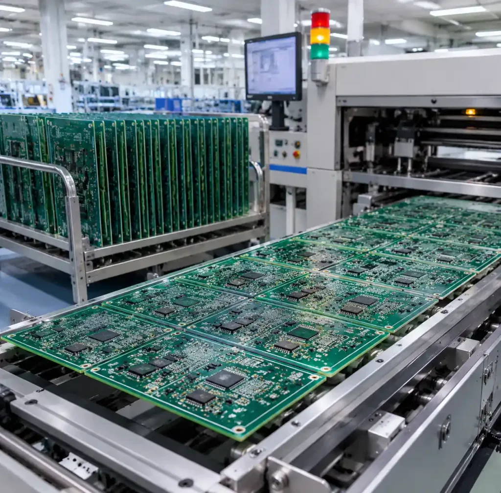
Production runs (500+ units) benefit from dedicated line time and optimized feeder setups. A 1000-unit order may complete in the same calendar time as a 100-unit job because line dedication eliminates queue delays between panels.
| Order Quantity | Setup Time | Production Time | Total Lead Time | Cost Impact |
|---|---|---|---|---|
| 10-20 units | 3-4 hours | 1-2 hours | 3-5 days | High per unit |
| 50-100 units | 3-4 hours | 4-8 hours | 5-7 days | Medium |
| 100-500 units | 3-4 hours | 1-2 days | 7-10 days | Medium-Low |
| 500+ units | 4-5 hours | 2-5 days | 10-20 days | Low per unit |
Frequently Asked Questions
How long does PCB assembly typically take?
Standard PCB assembly takes 10-15 days for boards with 4-8 layers and common components. Quick-turn services deliver in 3-7 days with expedite fees. Complex boards with 10+ layers or specialty materials require 3-6 weeks. Lead time starts after design files pass DFM review.
What is the difference between PCB fabrication time and assembly time?
PCB fabrication (bare board manufacturing) takes 3-10 days depending on layer count. Assembly includes component procurement (1-3 weeks for turnkey), SMT/THT placement (1-2 days), and testing (1-2 days). Total lead time is fabrication plus sourcing plus assembly plus test.
Can I reduce lead time without paying expedite fees?
Yes. Optimize your design for manufacturing with standard materials, common components, and IPC-compliant land patterns. Provide complete documentation, respond quickly to engineering questions, and submit orders 2-3 days before you need production to start. These practices reduce lead time by 25-40%.
What factors most commonly delay PCB assembly?
Component availability causes 40-60% of delays, especially for allocated ICs. Design issues requiring clarification add 1-3 days. Incomplete documentation delays order start. Testing failures from design violations trigger rework cycles that extend delivery by 1-3 days.
How does order quantity affect lead time?
Small batches (10-50 units) spend more time in setup. Large orders (500+ units) benefit from dedicated line time. Mid-volume orders (100-500 units) may wait for production capacity, extending lead time by 3-5 days.
What is quick-turn PCB assembly?
Quick-turn assembly delivers finished boards in 24 hours to 7 days instead of standard 10-20 day lead times. Services achieve this by running fabrication and component procurement in parallel and prioritizing your order. Expedite fees range from 30-100% premium.
Conclusion
PCB assembly lead time depends on four sequential phases: fabrication (3-10 days), component procurement (1-21 days), assembly (1-3 days), and testing (1-2 days). Understanding how layer count, material selection, component availability, and order quantity affect each phase lets you plan realistic timelines. DFM-optimized designs, complete documentation, and strategic component selection reduce lead time by 25-40% without expedite fees.
Andwin Circuits offers turnkey PCB assembly with 7-day quick-turn service for prototypes and 10-15 day standard lead time for production volumes up to 50 layers. Our IPC-A-610 Class 3 certified facility handles HDI, rigid-flex, and high-reliability assemblies for automotive, medical, telecommunications, and industrial applications worldwide.
Contact us today for PCB assembly quotes and lead time analysis.