
Copper Balancing in PCB: Preventing Warpage in Manufacturing
Over 40% of PCB warpage failures stem from unbalanced copper distribution during manufacturing. When boards arrive twisted or bowed at assembly, the root cause typically traces back to copper imbalance that locked in stress during lamination. Understanding copper distribution effects on flatness is critical to avoiding costly rework and assembly failures.
This guide explains copper-induced warpage physics, how to calculate copper balance during design, and proven strategies that keep boards flat. Learn more about our PCB manufacturing capabilities and rigid flex PCB solutions.
What Is Copper Balancing in PCB?
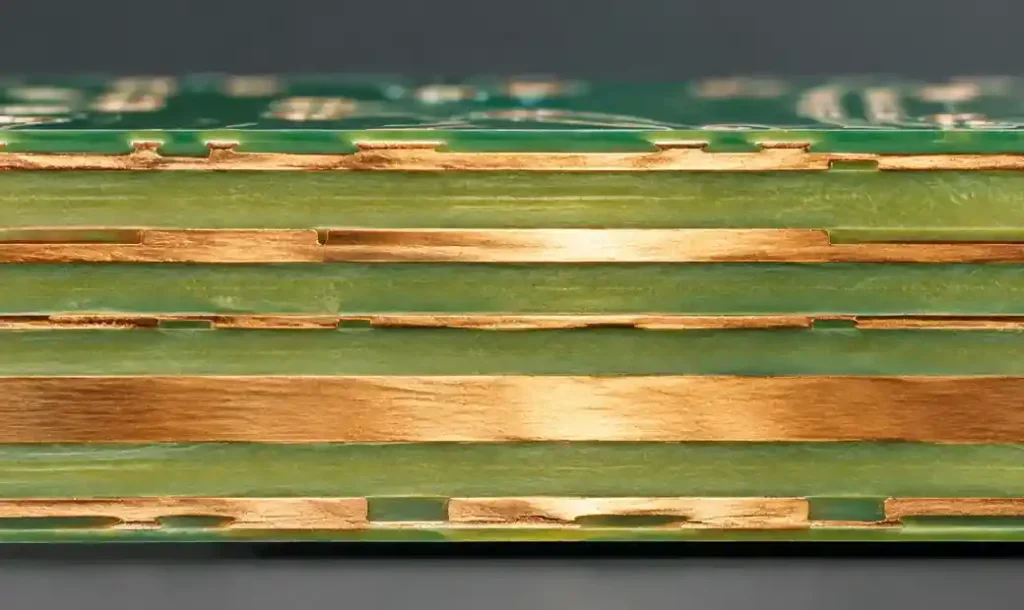
Copper balancing is the uniform distribution of copper across PCB layers to minimize internal stress during thermal processing. Balanced copper requires: similar coverage across paired layers, stackup symmetry from centerline, and no concentrated copper in one area while adjacent regions remain sparse.
Copper expands at 17 ppm/°C while FR-4 expands at 14-17 ppm/°C in-plane and 50-70 ppm/°C through thickness. During lamination at 170-180°C, materials heat together. Upon cooling, heavy copper areas contract more than light copper areas, creating permanent deformation when stress exceeds elastic limits.
How Copper Imbalance Causes Warpage
During lamination, prepreg resin flows at 170-180°C, bonding copper-clad core layers. As temperature rises, copper and substrate expand together. When cooling, uneven copper distribution—such as a 90% ground plane opposite 30% signal layer—generates asymmetric contraction. The heavy copper side pulls more than the light side, bending the board into bow or twist.
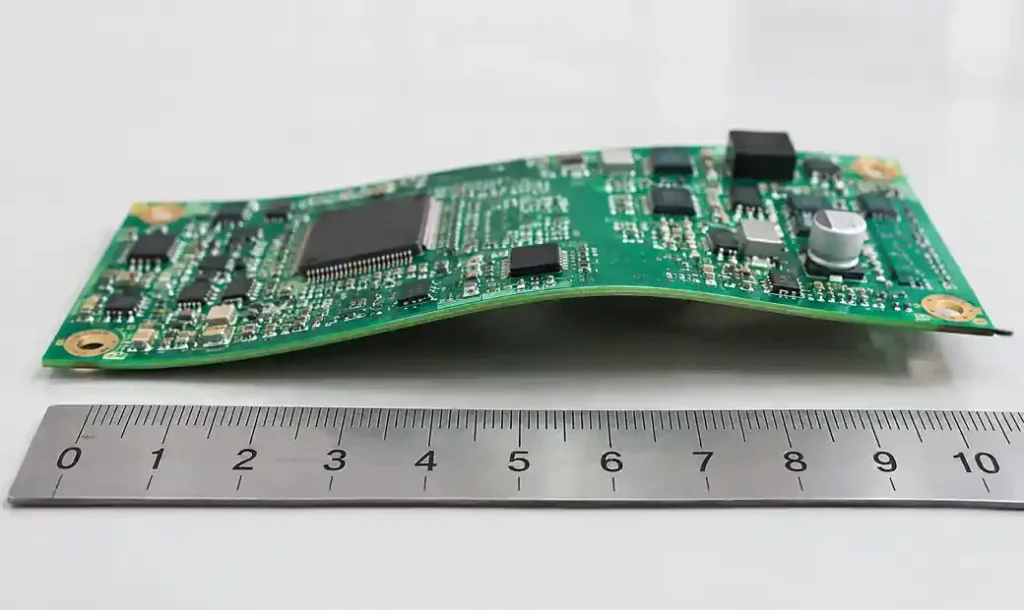
Bow describes cylindrical curvature with all corners coplanar. Twist occurs when one corner elevates while three contact a flat surface. IPC-TM-650 defines measurement: maximum deviation divided by diagonal length, expressed as percentage.
| Board Application | Maximum Bow/Twist (IPC-6012D) | Typical Production Target |
|---|---|---|
| SMT assembly, fine pitch components | ≤0.75% | ≤0.50% |
| Standard SMT assembly | ≤1.0% | ≤0.75% |
| Through-hole only, no SMT | ≤1.5% | ≤1.2% |
| Flexible and rigid-flex boards | ≤1.5% | ≤1.0% |
For a 200mm × 150mm board (241mm diagonal), 0.75% bow translates to 1.8mm maximum deviation. Boards exceeding specification cause pick-and-place head crashes, insufficient solder paste compression, and component tombstoning during reflow.
Calculating Copper Percentage
Copper percentage is copper area divided by total board area per layer. For manual verification: export Gerbers, import into CAD software with area measurement, calculate copper area (traces + pads + pours + planes), divide by board outline area, express as percentage.
Modern CAM systems calculate automatically. Target ranges:
| Layer Type | Target Copper Coverage | Acceptable Range |
|---|---|---|
| Signal layers (outer) | 35-50% | 30-60% |
| Signal layers (inner) | 30-45% | 25-55% |
| Power/ground planes | 75-95% | 70-98% |
| Mixed signal/plane layers | 50-70% | 45-75% |
| Layer-pair differential | ±10% ideal | ±20% maximum |
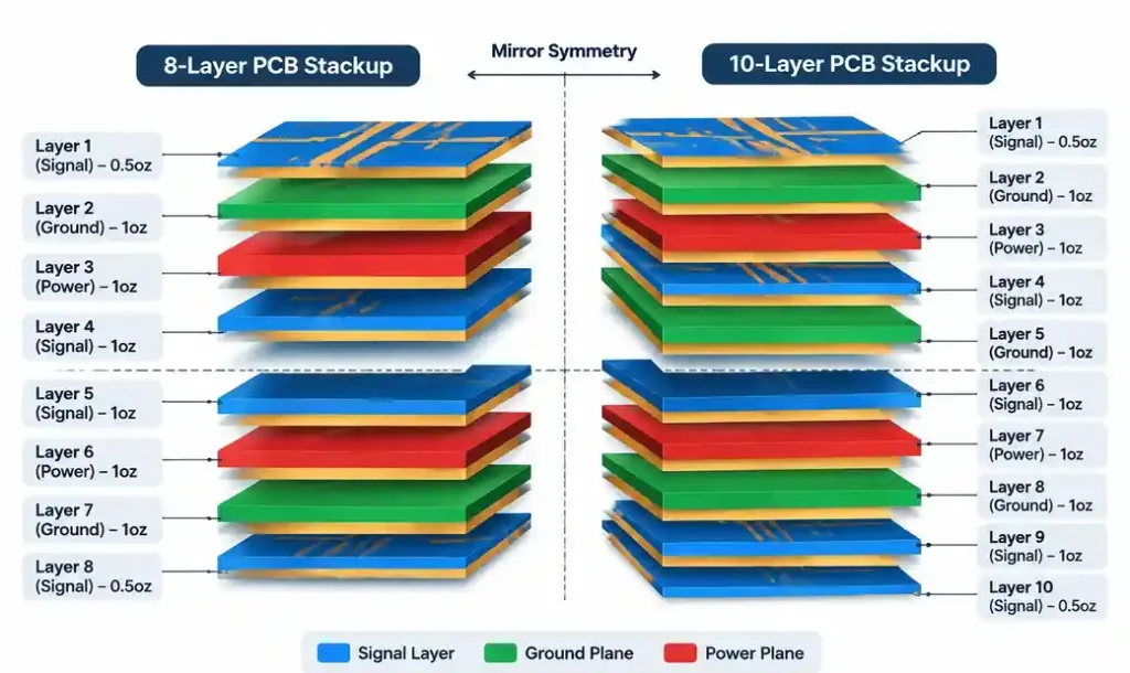
For symmetrical balance, mirror pairs around stackup centerline. In 8-layer boards: L1 matches L8 within ±10%, L2 matches L7, L3 matches L6, L4 matches L5.
Design Strategies to Prevent Warpage
Symmetrical Stackup Construction
Mirror-symmetric stackups prevent warpage most effectively. For 10-layer boards, construct from centerline:
- L1 (signal, 40%) ↔ L10 (signal, 40%)
- L2 (ground, 90%) ↔ L9 (ground, 90%)
- L3 (signal, 35%) ↔ L8 (signal, 35%)
- L4 (power, 85%) ↔ L7 (power, 85%)
- L5 (signal, 40%) ↔ L6 (signal, 40%)
Match copper weights between paired layers. Mixing 0.5oz on L2 with 2oz on L9 defeats symmetry. When high-current layers require heavy copper, apply identical weight to the mirrored position.
Copper Thieving Implementation
Copper thieving adds non-functional patterns to sparse regions, raising copper percentage without affecting circuits. Common patterns:
Dot Grids: 0.2-0.4mm pads at 0.8-1.5mm spacing provide ~15-25% additional coverage.
Hatched Fills: 0.15-0.3mm diagonal lines at 0.5-1.0mm spacing add 10-20% copper.
Polygon Islands: 1-3mm isolated shapes scattered in open areas.
Implementation rules:
- Maintain ≥0.4mm clearance from functional traces
- Connect thieving to ground via stitching vias (reduces EMI)
- Avoid RF-sensitive zones
- Use hatched patterns for high-frequency designs
Copper Pour Strategies
Hatched Pours: 45° or 90° hatching with 0.5-0.8mm width and 0.8-1.2mm spacing adds 35-50% coverage while maintaining etch uniformity and reducing capacitive coupling.
Solid Pours with Thermal Relief: For power/ground, use solid fill with thermal reliefs at pads (0.3-0.4mm spoke width, 4 spokes). Maintains coverage while enabling hand soldering.
Manufacturing Process Controls
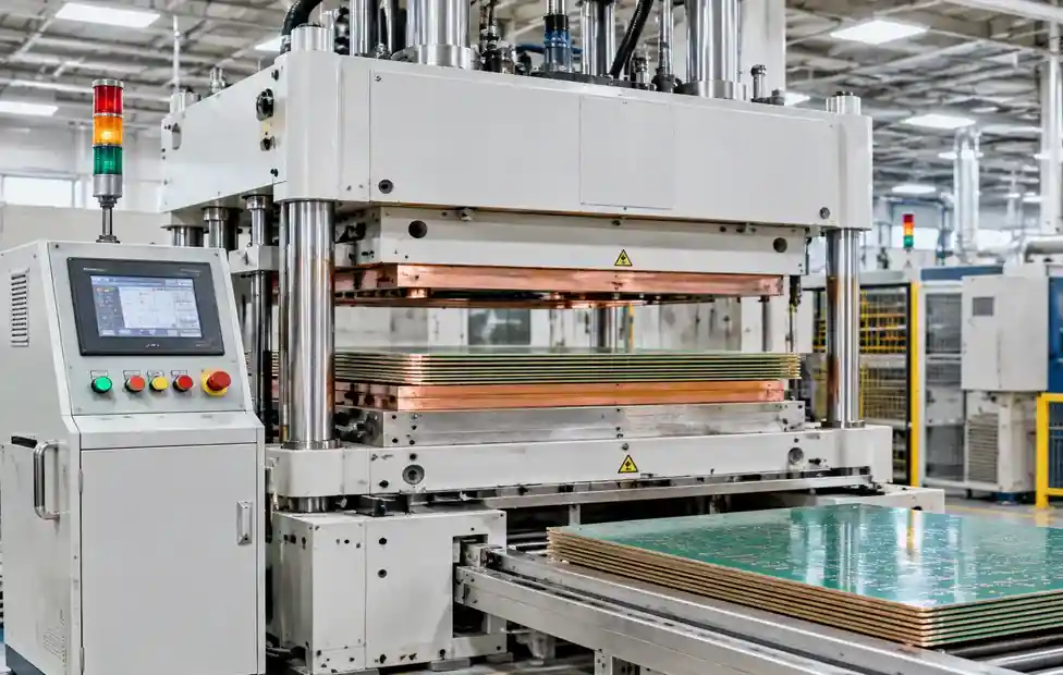
Proper lamination reduces warpage even when copper balance isn’t perfect. Critical parameters:
Heating Rate: Slow ramp (2-3°C/min) to 170°C allows uniform expansion. Rapid heating (>5°C/min) locks in stress.
Peak Temperature: 170-180°C for 60-90 minutes. Higher temperatures amplify CTE mismatch when copper is imbalanced.
Cooling Rate: Controlled 2-3°C/min prevents thermal shock and allows stress relaxation.
Pressure: 300-400 psi (2.1-2.8 MPa) typical. Higher pressure improves resin flow but increases compression stress.
Some manufacturers apply stress relief baking after lamination at 150-160°C for 2-4 hours, reducing warpage 20-30% in marginally imbalanced designs.
Troubleshooting Warpage Issues
After Lamination: Immediate warpage indicates primary copper imbalance. Check copper percentage per layer and pairing symmetry.
After Drilling/Routing: Mechanical stress reveals latent warpage. Use sharp bits and proper board support.
After Plating: Through-hole plating adds asymmetric copper. For >1oz plating, plate both outer layers simultaneously.
During Reflow: Warpage at 260°C peak indicates insufficient Tg margin. Specify high-Tg materials (170-180°C) for boards with copper imbalance.
| Warpage Level | Cause | Corrective Action |
|---|---|---|
| 0.3-0.5% | Minor imbalance | Add copper thieving to light layers |
| 0.5-0.8% | Layer pair mismatch | Rebalance paired layers to ±10% differential |
| 0.8-1.2% | Asymmetric stackup | Redesign for mirror symmetry |
| >1.2% | Severe imbalance | Full stackup redesign required |
Copper Balance Verification
Request detailed copper balance analysis from your fabricator. Professional CAM software generates reports showing per-layer copper percentage, paired-layer differentials, copper density heatmaps, and estimated warpage risk based on production data. Review during design phase, not after production failures.
For high-reliability applications (aerospace, medical, automotive), conduct FEA simulation modeling complete stackup with actual copper patterns, applying thermal loads representing lamination cycles. This identifies warpage risk before fabrication when rework costs thousands.
Application-Specific Considerations
HDI and High-Layer-Count Boards
High-density PCBs with 12-50 layers face amplified challenges. Multiple lamination cycles compound stress. Use thinner cores (0.1-0.2mm), sequential build-up with balanced layers, limit outer copper to 0.5-1oz, and apply thieving to every signal layer.
Andwin Circuits specializes in high-layer-count PCB manufacturing up to 50 layers with ≤0.50% bow/twist control.
Heavy Copper and Power Boards
Boards with 3-6oz copper for high-current applications require extra attention. Heavy copper increases thermal mass and exaggerates CTE mismatch. Use prepreg with higher resin content, apply heavy copper to symmetrically paired layers only, and consider metal core PCB alternatives for extreme power (10+ amps per trace).
Rigid-Flex PCBs
Flexible polyimide has different CTE than FR-4 rigid sections. Keep flex zone copper to 30-40% maximum, balance rigid section copper as standard multilayer, ensure flex-to-rigid transitions are symmetrically positioned, and avoid large pours crossing boundaries. Review rigid flex design guidelines for specifications.
FAQ
How much copper imbalance can PCB manufacturing tolerate?
Standard manufacturing handles ±20% copper differential between paired layers before warpage exceeds 0.75%. High-reliability applications require ±10% differential. Outer layer pairs (L1-Ln) are most critical because they experience maximum bending moment. Internal layer pairs have slightly more tolerance due to neutral axis positioning.
Does copper weight affect bow and twist independent of coverage percentage?
Yes. Heavier copper (2-3oz) creates larger absolute stress even at identical coverage percentages compared to standard 1oz copper. The thicker copper has greater thermal mass and higher contraction force. Always specify identical copper weights for mirrored layer pairs. If one layer requires 2oz for current capacity, either apply 2oz to the paired layer or add compensating copper elsewhere in the stackup.
Can warpage be corrected after manufacturing?
Limited correction is possible through controlled heating and flattening under pressure, but this risks delamination and only addresses stress-locked warpage, not underlying copper imbalance. Prevention through proper design is far more reliable and cost-effective than attempting post-process correction. Severely warped boards should be scrapped and the design corrected.
What is the impact of copper imbalance on electrical performance?
Beyond mechanical warpage, copper imbalance affects impedance consistency across a panel and board-to-board within a production run. Thicker copper regions have slightly lower impedance, creating variation in matched impedance pairs. For controlled impedance designs above 1 GHz, copper balance directly impacts signal integrity and insertion loss uniformity.
Conclusion
Copper balancing in PCB design is not a theoretical exercise—it’s a practical manufacturing requirement that directly impacts board flatness, assembly yield, and product reliability. The industry data is clear: copper imbalance accounts for over 40% of PCB warpage defects, and preventing these failures requires intentional design decisions during stackup planning and layout.
The key principles are straightforward: design mirror-symmetric stackups, match copper coverage between paired layers within ±10%, apply copper thieving to sparse layers, and verify balance through CAM reports before production. For complex boards with 10+ layers or heavy copper requirements, FEA simulation can predict warpage risk and guide optimization.
Andwin Circuits provides advanced PCB manufacturing capabilities up to 50 layers with strict bow and twist control ≤0.50% for high-reliability applications. Our engineering team works with customers during design phase to optimize copper balance, perform DFM analysis, and ensure flat boards in production. We support automotive, medical, telecommunications, and power electronics applications requiring tight tolerance control. Contact us for copper balance verification, stackup design consultation, and fast turnaround PCB manufacturing in 7-15 days.