
ESD Protection in PCB Design: Layout and Component Placement
Component-level ESD testing tells only half the story. ICs that pass 8kV HBM testing at the factory routinely fail at 2-4kV when assembled onto production boards. This disconnect stems from parasitic inductance, ground plane discontinuities, and poor component placement—factors invisible during chip-level qualification but dominant in real-world system performance.
In this article, we will examine the physical layout decisions that determine ESD immunity at the board level. This practical guide helps hardware engineers translate ESD specifications into actionable PCB design rules that deliver reliable field performance across automotive, industrial, and consumer applications.
Why Board-Level ESD Protection Fails
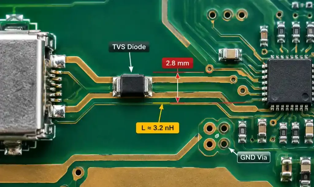
Standard TVS diodes spec clamping voltages of 6-12V, yet downstream ICs still suffer gate oxide damage during 8kV IEC 61000-4-2 testing. The root cause lies in parasitic inductance between the TVS and protected IC. During the <1ns ESD rise time, even 5nH of trace inductance generates 150V transient (V = L × di/dt with 30A peak current). This voltage spike bypasses the TVS entirely and appears directly at IC pins.
Real-world failure analysis reveals three critical design mistakes: TVS placement exceeding 10mm from connectors, single-via ground connections creating 1.5nH bottlenecks, and signal routing across split ground planes.
TVS Component Selection for PCB Integration
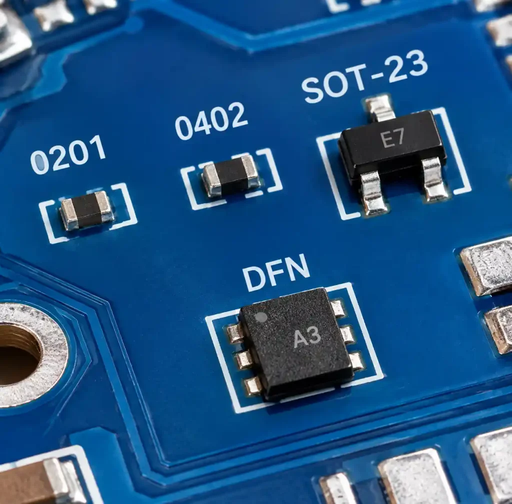
Choosing TVS protection requires balancing three electrical parameters. Working voltage (VRWM) must exceed maximum signal voltage by 15-20% to prevent false triggering. For 3.3V interfaces, specify VRWM minimum of 4.5V. Clamping voltage (VC) must stay below IC absolute maximum rating with 20% safety margin. Capacitance directly impacts high-speed signal integrity—USB 3.2 at 20Gbps requires <0.3pF, while HDMI 2.1 needs ≤0.25pF. Package size matters: 0201 packages minimize mounting inductance to <0.5nH versus 1.2nH for 0402.
| Interface Standard | Max Signal Voltage | Required VRWM | Max TVS Capacitance | Recommended Package |
|---|---|---|---|---|
| USB 2.0 (480 Mbps) | 3.6 V | 5.0-6.0 V | 5-10 pF | 0402 / SOT-23 |
| USB 3.2 Gen 2 (20 Gbps) | 3.6 V | 5.0-5.5 V | 0.3-0.5 pF | 0201 / DFN-6 |
| HDMI 2.1 (48 Gbps) | 3.6 V | 5.0-5.5 V | 0.2-0.3 pF | 0201 / uDFN |
| Ethernet 10GBASE-T | 2.5 V | 6.0 V | 15-25 pF | 0402 / SOT-23 |
| RS-485 | 5.0 V | 8.0-12.0 V | 50-100 pF | 0603 / SOD-323 |
| CAN Bus | 5.0 V | 8.0-12.0 V | 80-150 pF | 0603 / SOD-323 |
Bi-directional TVS diodes suit data lines where signal polarity reverses (USB, differential pairs), while unidirectional types work for power rails. Array packages integrate 4-8 channels with shared ground, reducing component count.
Critical Placement Rules for Low-Inductance Paths
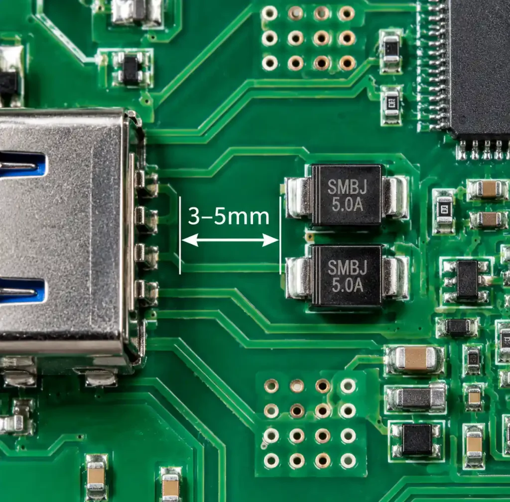
TVS placement follows the “first point of entry” principle: position protection between ESD entry point and downstream circuitry within 5mm of connector pins (routed distance). Every millimeter adds ~1nH parasitic inductance degrading protection.
Orient TVS ground pads toward the nearest ground connection. Route signal traces from connector to TVS input without vias or layer transitions. Ground connection requires 3-4 parallel 12-mil vias spaced 15-20 mils apart, reducing inductance from 1.5nH to <0.4nH. Position I/O connectors along board edges, creating an “ESD entry zone” with TVS components clustered near edge-mounted ground plane via fences.
Layout Techniques That Reduce Parasitic Inductance
Route traces between connector and TVS on the same layer without vias. Use 8-10 mil trace width maintaining 50Ω controlled impedance for RF interfaces. Adjacent ground traces or coplanar structure reduce loop inductance—place ground trace 2-3× trace width away, or use coplanar ground pours with 10-15 mil spacing.
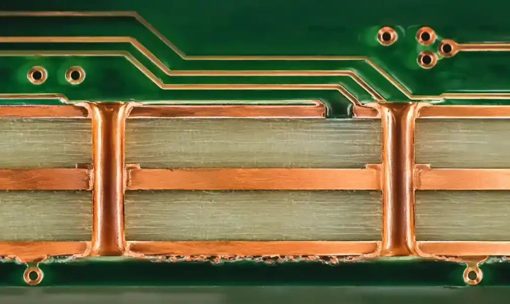
Via stitching at 40-50 mil intervals along board edges within 50-100 mils of edge cut provides uniform ground reference. For differential pairs (USB 3.x, HDMI, Ethernet), maintain 100Ω ±10% impedance with 5-8 mil pair spacing from connector through TVS to IC.
| Layout Technique | Inductance Reduction | Implementation Cost | Best Application |
|---|---|---|---|
| TVS within 5mm of connector | 60-70% vs 20mm placement | Low | All ESD-sensitive interfaces |
| 4-via parallel ground array | 70% vs single via | Low | High-current discharge paths |
| Adjacent ground trace routing | 40-50% vs isolated traces | Low | Single-ended signal protection |
| Coplanar ground pour | 50-60% vs isolated routing | Medium | Differential pair protection |
| Board edge via stitching | 30-40% overall improvement | Medium | Chassis-grounded enclosures |
Ground Plane Architecture for System-Level ESD Immunity
Solid continuous ground planes provide lowest impedance return paths. For 4-layer boards, dedicate layer 2 as solid ground. At plane splits, provide AC coupling through stitching capacitors (10-100nF) and vias at 20-25 mil spacing. Never route high-speed signals across splits—the return current discontinuity spikes loop inductance.
Connect PCB ground to chassis through multiple paths: mounting screws with star washers, dedicated ground tabs with multiple vias, or EMI gaskets along board edges.
Component-Level Protection Strategies Beyond TVS Diodes
Series termination resistors (22-100Ω) at IC outputs limit transient current di/dt. Place resistors within 5-10mm of driving IC, between IC and TVS, slowing ESD rise time from <1ns to 2-5ns.
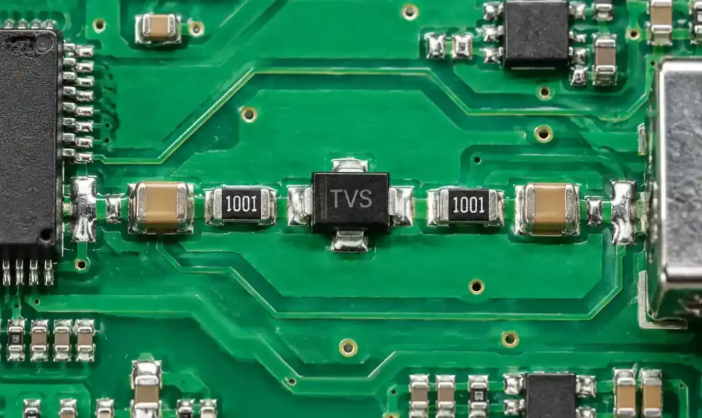
AC coupling capacitors (100nF-1µF) block DC ESD current while passing signals. Position between TVS output and IC input. Common-mode chokes on differential pairs provide 15-25dB attenuation—place after TVS. Ferrite beads (100-300Ω at 100MHz) on power rails suppress transients with local bypass capacitors.
Design Rules for Specific Interface Standards
USB 2.0 requires bidirectional TVS on D+/D- (5-10pF) plus VBUS, positioned within 3mm of connector. USB 3.x needs <0.5pF ultra-low capacitance arrays. Add 27Ω series resistors for additional protection.
HDMI 2.1 needs 0.2-0.3pF TVS arrays maintaining 100Ω differential impedance through protection. Ethernet 10/100BASE-T uses 15-25pF TVS with 1500W rating, while 10GBASE-T requires <3pF. Add 75Ω series resistors at magnetics center taps.
| Interface Type | Signal Count | TVS Topology | Max Capacitance | Additional Protection |
|---|---|---|---|---|
| USB 2.0 | 2 data + VBUS | Bi-directional array | 5-10 pF | 27Ω series resistors |
| USB 3.2 Gen 2 | 4 SuperSpeed + 2 USB 2.0 | Dual array (low-C SS) | 0.3-0.5 pF SS, 5 pF USB 2.0 | Common-mode choke |
| HDMI 2.1 | 4 TMDS pairs + 3 aux | Integrated 13-channel array | 0.2-0.3 pF | AC coupling caps |
| Ethernet 10GBASE-T | 4 differential pairs | 8-line array at magnetics | 2-5 pF | 75Ω CM termination |
| CAN Bus | 2 (CAN_H/CAN_L) | Bi-directional | 80-120 pF | Split termination network |
Testing and Validation Procedures

ESD testing per IEC 61000-4-2 uses calibrated simulators (8kV contact, 15kV air discharge) applied to every connector pin and exposed surface. Apply 25 discharges per test point at 1-second intervals. Test at Level 3 (6kV) for commercial products, Level 4 (8kV) for industrial and automotive.
Test at temperature extremes and voltage limits. When failures occur, TDR measurements map impedance discontinuities, while thermal imaging shows current paths. Destructive analysis reveals junction melting and gate oxide puncture patterns.
Application Requirements for Harsh Environments
Automotive electronics face severe ESD per ISO 7637-2 and ISO 10605 (8kV contact, 25kV air discharge). Meet these requirements through AEC-Q101 qualified TVS components and chassis-grounded enclosure design.
Industrial systems need Level 4 testing (6-8kV) plus EFT per IEC 61000-4-4, requiring 5000W pulse TVS diodes. Industrial applications benefit from conformal coating over protection zones. Medical devices follow IEC 60601-1-2 (6kV contact) with redundant protection on patient-isolated interfaces per medical PCB standards.
High-Speed Signal Integrity with ESD Protection
ESD protection on multi-gigabit interfaces requires preserving signal eye diagrams while clamping nanosecond transients. TVS capacitance creates impedance mismatches affecting signal quality. Controlled impedance design must account for TVS parasitics in channel budgets.
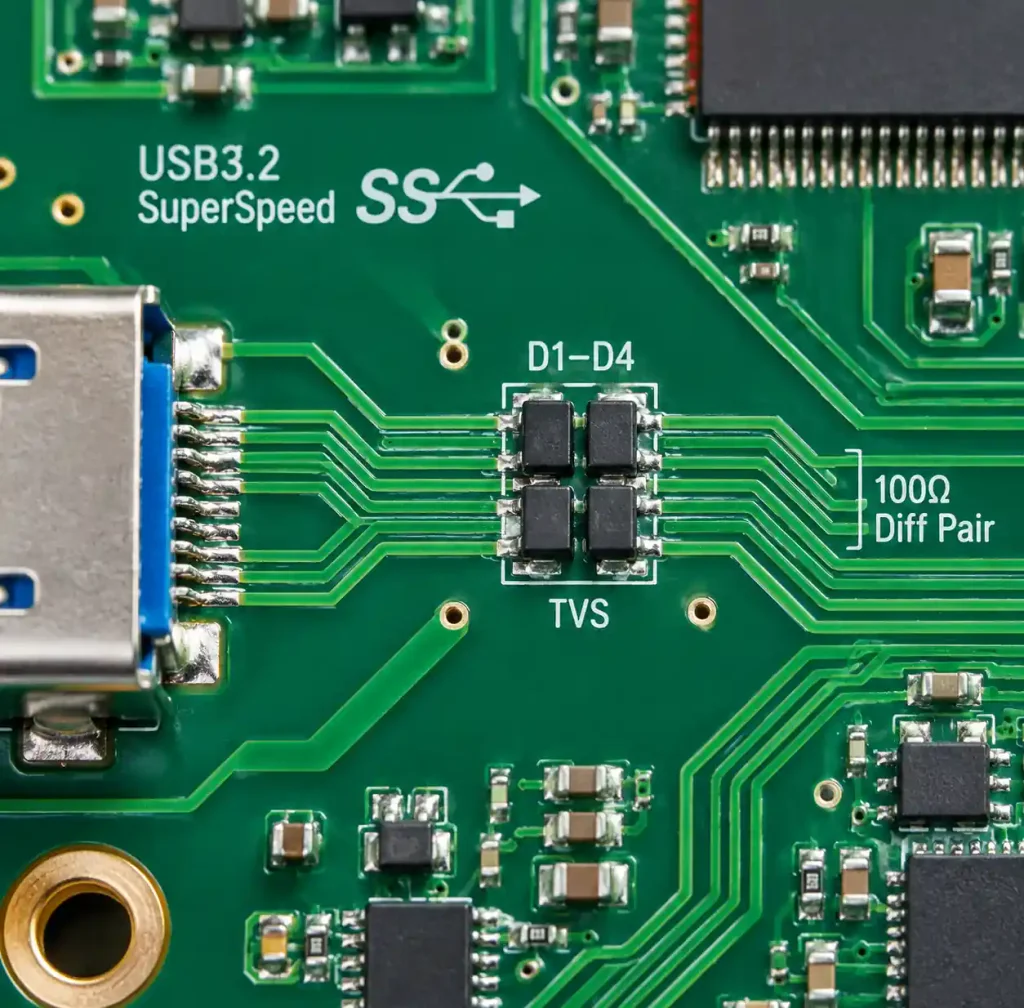
For PCIe Gen 4 (16GT/s), specify TVS ≤0.5pF and maintain 100Ω ±10% impedance through protection. Use SPICE models to validate eye mask compliance before fabrication. RF interfaces (Wi-Fi, cellular) demand <0.3pF capacitance to avoid antenna detuning.
Implementation Checklist and Best Practices
Cluster external connectors along board edges near ground via fences. Verify ground plane integrity using field solver analysis. Check for splits beneath high-speed traces and TVS components. Review signal flow: connector → TVS → series elements → protected IC. Confirm 20-30% TVS clamping margin versus IC ratings. Budget 2-4 iterations for high-speed multi-interface designs through testing refinement.
FAQ
How close should TVS diodes be to connectors?
Within 5mm routed distance from connector pins to TVS input. Each millimeter adds ~1nH parasitic inductance generating voltage spikes during ESD events. For Level 4 testing, reduce to 3mm maximum.
What via configuration provides lowest ground inductance?
Use 3-4 parallel 12-mil vias spaced 15-20 mils apart, connecting TVS ground pad to solid ground plane, reducing inductance from 1.5nH to 0.3-0.4nH.
Can one TVS protect multiple connectors?
No. Each connector requires dedicated TVS within 5mm to minimize discharge path inductance, unless connectors are within 5mm of each other.
How to select TVS capacitance for USB 3.2?
USB 3.2 Gen 2 (20Gbps) requires ≤0.5pF per differential pair on SuperSpeed lanes. USB 2.0 signals tolerate 5-10pF. Use dual arrays with ultra-low capacitance for high-speed lanes.
Does conformal coating affect ESD performance?
Conformal coating improves ESD immunity by increasing surface breakdown voltage without affecting TVS clamping. Ensure 25-125µm thickness per IPC-CC-830.
Conclusion
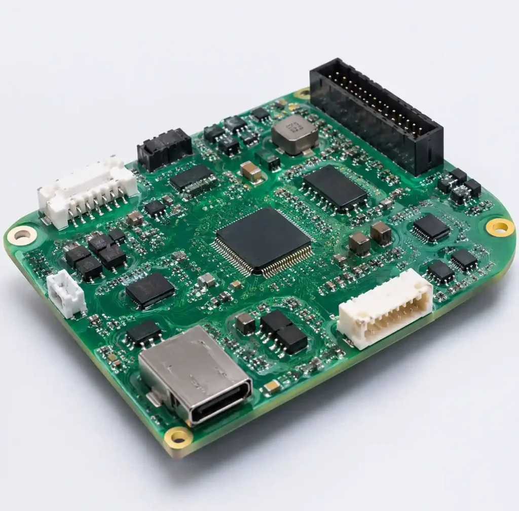
Effective board-level ESD protection requires systematic integration of component selection, physical placement, and layout topology. Success depends on minimizing parasitic inductance through sub-5mm TVS-to-connector spacing, parallel via ground connections, and continuous ground plane architecture. These design decisions determine whether protection components deliver their rated performance or fail due to layout-induced voltage spikes.
Testing and validation at the board level reveal protection weaknesses invisible during component qualification. Budget for iterative design refinement based on ESD test results, particularly for automotive and industrial applications where field reliability demands exceed consumer product requirements. Proper implementation protects both product functionality and brand reputation against the costly field failures that ESD events create.
If you need high-quality PCB manufacturing for automotive, industrial, or medical applications with rigorous ESD protection requirements, Andwin Circuits offers advanced PCB manufacturing capabilities up to 50 layers with fast turnaround in 7 days. Our facility maintains ISO 9001, IATF 16949, and UL certifications for industries where ESD immunity directly impacts product reliability and safety. We have successfully delivered PCB assembly services for automotive ADAS systems, industrial control equipment, and medical devices requiring IEC 61000-4-2 Level 4 compliance.
Contact us today for custom PCB solutions with design-for-ESD review services and competitive factory-direct pricing for your next project.