Andwin HDI multilayers PCB:Injecting Core Power into High-End Electronics
Within the precision of microvias lies the limitless potential for technological breakthroughs.
In today’s world of increasingly thinner,lighter,and more powerful electronic devices,high-end applications place increasingly stringent performance demands on electronic components.Traditional PCBs can no longer meet the extreme pursuit of stability,efficiency,and miniaturization by”ultra-high-performance integrated circuits “
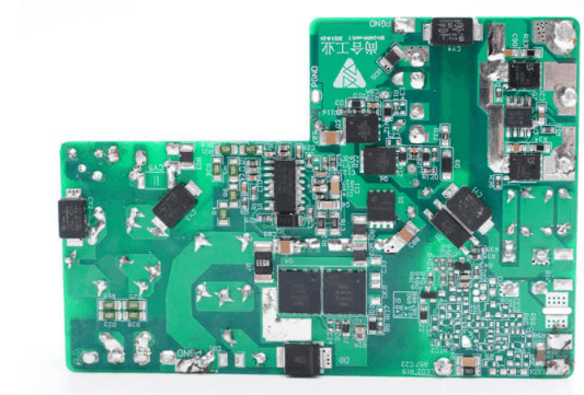
High-density interconnect(HDI)technology has become an inevitable trend in the PCB industry,and Andwin HDI multilayer PCBs are outstanding representatives of this technology,Through”microvia design,high-density wiring”and”advanced stack-up structure”,they provide powerful support for the next generation of high-end electronic products.
1.What is an HDI multilayer PCB?
High-density interconnect(HDI)PCBs are circuit board with high circuit density that utilize mirco-blind buried via technology.
Compared to traditional PCBs,HDI PCBs can accommodate”more components with the same area”.enabling more compact designs and more powerful functions.
HDI multilayer board utilize”micro-blind vias and buried vias to reduce the number of vias ,increase wiring density and achieve finer circuit layouts.
Currently,HDI boards have evolved from simple first-order designs to complex multi-order and arbitray-layer interconnect structures,meeting the needs of various application scenarios.
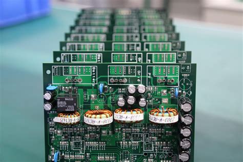
2.Andwin HDI Multilayer PCB technical Advantages
Ultra-high Density Interconnection,unleashing Limitless potential
Andwin HDI multilayer PCBs employ “advanced stack-up structures and microvia technology to achieve finer circuit layouts and higher wiring density
Our product support”blind via,buries vias,and other design”,result in smaller foot prints and aligning with the trend towards thinner ,smaller,and more portable electronic device.
Superior Electrical Performance,stable and Reliable
Through optimized stack-up structures and impedance control,Andwin HDI boards effectively”reduce signal loss and crosstalk,improving signal transmission speed and intergrity.
We select high-quality materials and combine them with precise manufacturing process to ensure that our circuit boards posses “Superior signal transmission integrity,anti-interference capabilities,and thermal stability ,enabling stable operation even in harsh working environments.
Diverse Stack-up Designs to Meet Complex Needs
Andwin HDI boards offer a diverse range of stack-up options,from”first-order to third-order,and even arbitary layer interconnects,to meet the complex needs of different customers
Whether it’s a standard 8-10 layer design or a highly complex struture with more than 10 layers,we can provide a perfect solution.
3.Application Areas of Andwin HDI Multilayer PCBs
Artifical Intelligence and Machine learning
In the fields of AI and machine learing,Andwin HDI Boards provide AI chips with “high-speed,stable data transmission channel”helping AI applications overcome performance bottlenecks.
Whether it’s AI servers or terminal intelligent devices,our HDI boards provide excellent performance support.
5G Communication and IOT
Our HDI board meet the”high-frequency,high-speed signal transmission requirements of 5G base stations and IOT devices”,building an intelligent world of interconnected things.
In the field of communication infrastructure,Andwin HDI board ensure the stability and reliability of data transmission thank to their superior signal interfrity.
Automotive Electronic and Medical Devices
Andwin HDI board provide high-performance high-reliability circuit solutions for”medical devices and automotive electronic system,safeguarding lives and travel safety.
In the automotive electronic field,our products are used to achieve complex circuit layouts and high-density intergation,such as “autonomous driving systems and intelligent driving assistance systems and intelligent driving assistance systems.
Consumer Electronics and Data Centers
In the consumer electronics field,Andwin HDI boards help smartphones,tablet,and other devices achieve the design goal of”smaller size and higher performance.
Our products are also widely used in”artificial intelligence,cloud computing,and other data center fileds”,providing reliable support for high-speed computing.
4.Andwin’s Core Competenices
Professional Technical Team and Extensive Industry Experience
We have an experienced technical team that provides customers with”professional technical support and customized solutions.
Andwin has deep technical expertise in the HDI field and can provide the most suitable product solutions base on the specific needs of our customers.
Advanced Production Equipment and Processes
We have introduced advanced production equipment,combined with advanced processes such as”Microvia design and high-density wiring”to ensure stable and reliable product solutions based on the specific needs of our customers.
Advanced Production Equipment and Processes
We have introduced advanced production equipment,combined with advanced processes such as :microvia design and high-density wiring,to ensure stable and reliable product quality.
Whether it’s”thin HDI(0.3~1.0mm)or thick HDI(2.0~5.5mm),we have entered a stable mass production stage.
Strict Quality Control System
Andwin has established a comprehensive quality management systerm,achieving multiple certifications including”ISO9001 and IATF16949″providing customers with peace of mind.
From raw material procurement to manufacturing,every step is strictly controlled to ensure the superior performance and high reliability of the final product.
5.Market Prospect and Development Trends
According to market research data,the global multilayer HDI PCB market sales are projected to reach 90.12 billion yuan,with a “compound annual growth rate(GAGR)of 5.3%(2025-2031)
Meanwhile, another report shows that the global HDI Board market size reached US$9.643 billion in 2024 and is projected to grow to US$13.85 billion by 2031, with a CAGR of 5.4%.
The Chinese market has seen rapid changes in recent years and is expected to maintain stable growth in the coming years,primarily due to the rapid development of emerging technologies such as”5G Comunication,artifical intelligence,and the Internet of Things”.
Faced with this vast market prospect Andwin will continue to increase its R&D investment and continuously improve product performance to meet the growing market demand.
In the highly competive HDI PCB market ,Andwin means choosing a “reliable efficent,and professional solution”let’s work together to inject core power into your electronic products and create a technological future.
Whether you are in the fields of artificial intelligence,5G communication ,automotive electronics or medical devices,Andwin HDI multilayer PCBs are the ideal choice for breaking through design bottlenecks and creating superior products.


