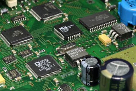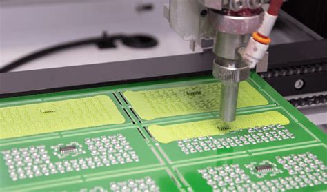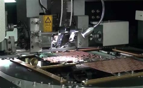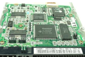
UV laser application in various PCB materials
Ultraviolet lasers are the best choice for a variety of PCB materials in many industrial applications, from the most basic circuit boards, circuit wiring, to advanced processes such as pocket-sized embedded chips. The variability of this material makes UV lasers the best choice for a wide range of PCB materials in many industrial applications, from…