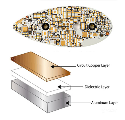
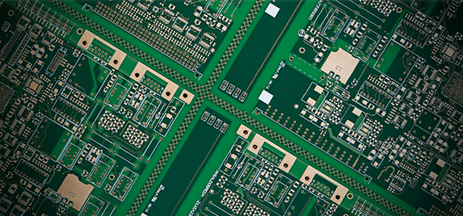
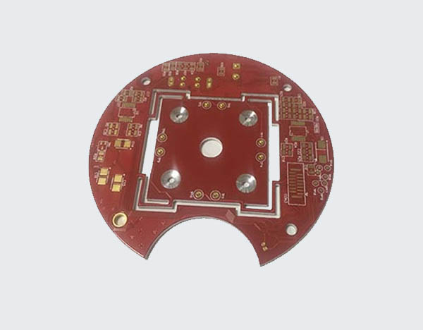
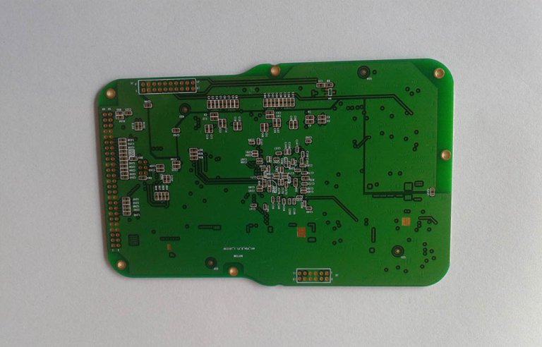
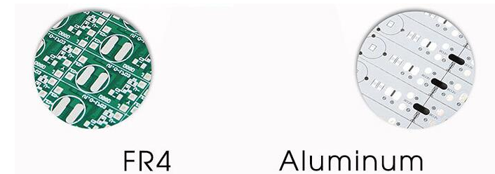
Ceramic inlay pcb
Ceramic inlay PCBs have emerged as a pivotal innovation in the realm of high-frequency applications, offering a multitude of advantages that make them indispensable in various advanced technological fields.

Ceramic inlay PCBs have emerged as a pivotal innovation in the realm of high-frequency applications, offering a multitude of advantages that make them indispensable in various advanced technological fields.

Ceramic capacitors are fundamental components in the realm of electronics, particularly in printed circuit boards (PCBs). These capacitors are widely appreciated for their reliability, compact size, and cost-effectiveness.
To understand the basics of ceramic capacitors, it is essential to delve into their construction, functionality, and applications.

Designing optimal PCB footprints for ceramic capacitors is a critical aspect of ensuring the reliability and performance of electronic circuits. Ceramic capacitors, known for their stability, low cost, and wide range of values, are ubiquitous in modern electronics.
However, the effectiveness of these components is heavily influenced by the design of their printed circuit board (PCB) footprints.
A well-designed footprint not only facilitates proper soldering and placement but also minimizes potential issues such as parasitic inductance and capacitance, which can adversely affect circuit performance.

Ceramic base printed circuit boards (PCBs) have emerged as a pivotal technology in the realm of high-frequency applications, offering a multitude of advantages that make them indispensable in various advanced electronic systems.

Building a circuit board is a meticulous process that requires a combination of precision, patience, and the right set of tools and materials. To ensure a successful project, it is essential to gather all necessary components before beginning. This preparation not only streamlines the workflow but also minimizes the risk of errors and rework.

When it comes to optimizing PCB layout, there are several essential tips that can significantly enhance the performance, reliability, and manufacturability of your printed circuit board.

Top Online PCB Manufacturers for High-Quality Prototypes When it comes to developing high-quality prototypes, selecting the right online PCB manufacturer is crucial. The market is replete with numerous options, each offering a unique set of services and capabilities. However, a few stand out due to their commitment to quality, customer service, and technological innovation. Among…

When embarking on DIY electronics projects, selecting the right circuit board is crucial for both the functionality and success of your endeavor.
The market offers a plethora of options, each with unique features and benefits tailored to various applications. To assist you in making an informed decision, we have compiled a list of the top 10 circuit boards that stand out for their quality, versatility, and ease of use.

When designing a 4-layer printed circuit board (PCB), achieving optimal signal integrity is paramount. Signal integrity refers to the quality and reliability of electrical signals as they travel through the PCB. A well-thought-out stackup can significantly enhance signal integrity, reduce electromagnetic interference (EMI), and improve overall performance. Therefore, understanding the best practices for a best 4 layer PCB stackup is essential for engineers and designers.

Bergquist Metal Core PCBs (Printed Circuit Boards) have emerged as a pivotal innovation in the realm of high-power applications, offering a multitude of advantages that make them indispensable in various industries.
These PCBs are specifically designed to manage and dissipate heat more effectively than traditional FR4 boards, which is crucial in high-power environments where thermal management is a significant concern. The unique construction of Bergquist Metal Core PCBs, which typically includes a metal substrate, a thermally conductive dielectric layer, and a copper circuit layer, provides a robust solution to the challenges posed by high-power applications.

Bendable metal core printed circuit boards (PCBs) represent a significant advancement in the field of modern electronics, offering a range of advantages that cater to the evolving demands of contemporary technology. These innovative PCBs are designed with a metal core, typically aluminum or copper, which provides enhanced thermal management and mechanical stability. The ability to bend these PCBs without compromising their structural integrity or performance opens up new possibilities for electronic device design and functionality.
Innovations In Benchmark PCB Manufacturing Techniques Benchmark PCB manufacturing has undergone significant advancements in recent years, driven by the need for higher performance, greater reliability, and more efficient production processes. One of the most notable innovations in this field is the development of high-density interconnect (HDI) technology. HDI PCBs are characterized by their finer lines…

Benchmark PCB manufacturing has undergone significant advancements in recent years, driven by the need for higher performance, greater reliability, and more efficient production processes. One of the most notable innovations in this field is the development of high-density interconnect (HDI) technology.

Bed of nails PCB assembly testing, also known as in-circuit testing (ICT), is a method that has gained significant traction in the electronics manufacturing industry due to its numerous benefits.
This testing technique involves the use of a fixture, often referred to as a “bed of nails,” which contains an array of spring-loaded pins. These pins make contact with specific test points on a printed circuit board (PCB) to evaluate its functionality and integrity.

When designing high-speed, high-frequency printed circuit boards (PCBs), the selection of dielectric materials is a critical factor that significantly influences the performance and reliability of the final product.
The dielectric material, which serves as an insulating layer between conductive traces, plays a pivotal role in determining the signal integrity, impedance control, and overall electrical performance of the PCB.
As the demand for faster data transmission and higher operational frequencies continues to grow, engineers must carefully evaluate the properties of various dielectric materials to ensure optimal functionality.