9 pin pcb connector
Application and Selection Guide of 9 Pin PCB Connectors 9 Pin PCB connectors play a vital role in modern electronic…
Application and Selection Guide of 9 Pin PCB Connectors 9 Pin PCB connectors play a vital role in modern electronic…
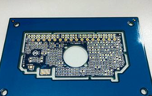
The design and application of 9-pin ceramic tube socket PCB is of great significance in the field of electronic engineering. First of all, it is crucial to understand the basic structure and function of the 9-pin ceramic tube socket. Ceramic tube sockets are usually used for the connection of vacuum tubes and electron tubes, and are favored for their excellent heat resistance and electrical insulation properties. The 9-pin design provides more connection options and is suitable for complex circuit requirements.
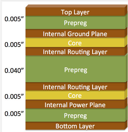
the 8 layer PCB stackup design is of great significance in modern electronic design. Through reasonable interlayer configuration and layout, signal integrity and power stability can be effectively improved, and electromagnetic interference can be reduced, thus achieving high-performance electronic product design

With the continuous development of electronic products, the requirements for PCB are getting higher and higher. Especially for some complex electronic products, such as high-performance computers, communication equipment, etc., multi-layer boards are often needed to meet their complex wiring requirements. Among these multi-layer boards, 8-layer boards are more common. So, for the stacking structure of PCB 8-layer boards, what is the 8 layer pcb thickness
8 layer PCB prototype design is a complex and delicate process, and each step requires the designer’s meticulousness and expertise. By strictly following the design process and paying attention to key details, designers can ensure that the final circuit board has excellent performance and reliability.
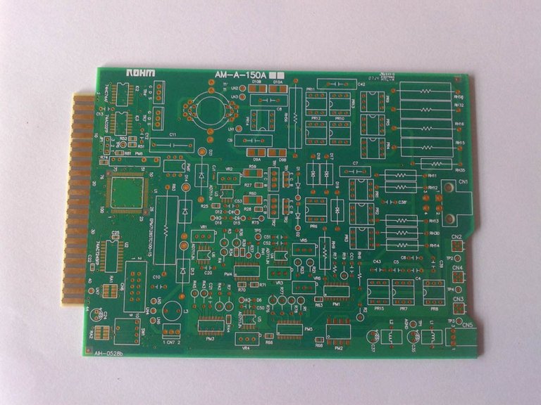
the design and manufacturing process of 8 layer PCB motherboard is a multi-step, precise and complex process. Each link requires a high degree of expertise and technical support, from design, material selection to manufacturing and quality control, each step is crucial. Through scientific and reasonable design and strict manufacturing process, high-performance and high-reliability 8-layer PCB motherboards can be produced to meet the needs of various complex electronic devices.

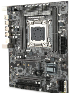
building an 8 bit computer PCB requires detailed planning and execution of multiple links from component selection, circuit design, PCB layout, electrical rule checking to final manufacturing. Each link needs to be carefully considered and processed to ensure that the final PCB can meet the design requirements and work properly. Through a systematic design process and strict quality control, a high-performance 8-bit computer PCB can be successfully built.
7 Series PCB Design Guide: Tips and Techniques for Optimizing Signal Integrity When designing 7 series PCBs, optimizing signal integrity…
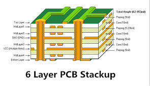
he best practices for 6-layer PCB stacking design include reasonable hierarchy, optimized signal layer layout, good power and grounding design, appropriate use of vias, and effective thermal management. By following these best practices, the performance and reliability of the circuit board can be significantly improved to meet the needs of high-performance applications.

the selection and application of 6 Pin PCB connectors requires comprehensive consideration of electrical performance, mechanical performance, environmental factors, and actual application requirements. Through reasonable selection and correct use, the reliability and performance of electronic equipment can be improved to ensure its stable operation in various environments.
6 layer pcb stackup for high speed y applications requires comprehensive consideration of multiple factors such as signal integrity, power stability, and electromagnetic compatibility. Excellent performance of high-frequency circuits can be ensured through reasonable stacking structure, fine signal layout, tight power and ground coupling, careful use of vias, and effective simulation and testing.simulation and testing.
It is crucial to understand the key steps and precautions when designing a 6 layer PCB prototype First, the designer…

The design and manufacturing process of 6 ayer PCB motherboard is a complex and sophisticated process involving multiple steps and technical details.
Analysis of the key steps and technical points of 6-layer PCB manufacturingThe manufacturing process of 6-layer printed circuit boards (PCBs) is complex and delicate, involving multiple key steps and technical points.
We use cookies to improve your experience on our site. By using our site, you consent to cookies.
Manage your cookie preferences below:
Essential cookies enable basic functions and are necessary for the proper function of the website.
Statistics cookies collect information anonymously. This information helps us understand how visitors use our website.
Google Analytics is a powerful tool that tracks and analyzes website traffic for informed marketing decisions.
Service URL: policies.google.com (opens in a new window)
SourceBuster is used by WooCommerce for order attribution based on user source.
You can find more information in our privacy policy and privacy policy.