
Automated Optical Inspection (AOI) in PCB Manufacturing: A Comprehensive Guide
Introduction
In the fast-evolving electronics industry, Printed Circuit Boards (PCBs) are the backbone of nearly all electronic devices. As PCBs become more complex with higher component density and finer pitch, ensuring their quality and reliability is critical. Automated Optical Inspection (AOI) has emerged as a vital technology in PCB manufacturing, enabling high-speed, high-precision defect detection. This article explores the role of AOI in PCB production, its benefits, challenges, and future trends.
1. What is AOI in PCB Manufacturing?
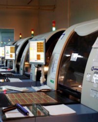
Automated Optical Inspection (AOI) is a non-contact, image-based inspection method used to detect defects in PCBs during and after the manufacturing process. AOI systems utilize high-resolution cameras, advanced lighting techniques, and sophisticated algorithms to compare PCB images against design specifications or known good boards.
Key Applications of AOI in PCB Production:
- Solder Paste Inspection (SPI): Verifies the correct application of solder paste before component placement.
- Pre-Reflow Inspection: Checks component placement accuracy before soldering.
- Post-Reflow Inspection: Identifies soldering defects such as bridges, insufficient solder, or misaligned components.
- Final PCB Inspection: Ensures overall board quality before shipment.
2. How AOI Works in PCB Inspection
The AOI process involves several key steps:
Step 1: Image Capture
- High-resolution cameras capture images of the PCB from multiple angles.
- Different lighting techniques (e.g., coaxial, side, or UV lighting) highlight various defects.
Step 2: Image Processing
- Advanced algorithms analyze the captured images.
- Machine vision software compares the PCB against a reference design or golden sample.
Step 3: Defect Detection
- The system flags discrepancies such as missing components, misalignment, solder defects, or scratches.
- Defects are classified based on severity (critical, major, minor).
Step 4: Reporting & Feedback
- Inspection results are logged for quality control and process improvement.
- Defective boards are flagged for rework or rejection.
3. Advantages of AOI in PCB Manufacturing
1. High Accuracy & Precision
- AOI systems can detect defects as small as 10 microns, ensuring high-quality PCB production.
- Reduces human error compared to manual inspection.
2. Increased Throughput
- AOI machines inspect hundreds of PCBs per hour, significantly faster than manual checks.
- Ideal for high-volume manufacturing environments.
3. Early Defect Detection
- Identifies issues early in production (e.g., solder paste defects before reflow), reducing scrap costs.
4. Data-Driven Process Improvement
- AOI generates detailed reports, helping manufacturers identify recurring defects and optimize processes.
5. Compliance with Industry Standards
- Ensures compliance with IPC-A-610 and other quality standards.
4. Common Defects Detected by AOI
AOI systems can identify a wide range of PCB defects, including:
| Defect Type | Description |
|---|---|
| Missing Components | Components not placed on the PCB. |
| Misaligned Components | Components shifted from their intended positions. |
| Solder Bridges | Unintended solder connections between pads. |
| Insufficient Solder | Poor solder joints leading to weak connections. |
| Excess Solder | Too much solder causing potential shorts. |
| Wrong Polarity | Components placed in reverse orientation. |
| Scratches & Contamination | Physical damage or foreign material on the PCB. |
5. Challenges & Limitations of AOI
Despite its advantages, AOI has some limitations:
1. False Positives & Negatives
- Overly sensitive systems may flag acceptable variations as defects (false positives).
- Certain defects (e.g., hidden solder joints under components) may go undetected (false negatives).
2. High Initial Investment
- Advanced AOI systems require significant capital expenditure.
3. Programming Complexity
- Setting up inspection parameters for new PCB designs can be time-consuming.
4. Limited 3D Inspection Capability
- Traditional AOI is primarily 2D; 3D inspection requires additional technologies like Automated X-ray Inspection (AXI).
6. AOI vs. Other PCB Inspection Methods
| Inspection Method | Pros | Cons |
|---|---|---|
| Manual Inspection | Low cost, flexible. | Slow, prone to human error. |
| AOI | Fast, high accuracy, scalable. | Limited to surface defects, false positives. |
| AXI (Automated X-ray Inspection) | Detects hidden defects (e.g., BGA solder joints). | Expensive, slower than AOI. |
| In-Circuit Testing (ICT) | Tests electrical functionality. | Requires physical probes, limited to post-assembly. |
For comprehensive quality control, manufacturers often combine AOI with AXI and ICT.
7. Future Trends in AOI Technology
1. AI & Machine Learning Integration
- AI-powered AOI systems improve defect recognition and reduce false calls.
- Self-learning algorithms adapt to new PCB designs faster.
2. 3D AOI for Advanced Packaging
- Enhanced 3D imaging detects complex defects in high-density interconnects (HDI) and miniaturized components.
3. Inline AOI with Smart Factories
- Integration with Industry 4.0 and IoT enables real-time process adjustments.
4. Higher Resolution & Faster Processing
- Advances in camera technology allow for faster inspections with micron-level precision.
8. Conclusion
AOI is an indispensable tool in modern PCB manufacturing, ensuring high-quality production while reducing costs and defects. As technology evolves, AI-driven AOI, 3D inspection, and smart factory integration will further enhance its capabilities. While challenges like false positives and high initial costs persist, the benefits of AOI far outweigh its limitations, making it a cornerstone of efficient and reliable PCB manufacturing.
By adopting AOI, electronics manufacturers can achieve higher yields, lower rework costs, and improved product reliability—key factors in staying competitive in the fast-paced electronics industry.