
Blind and Buried Via PCB Design Rules: T/D Ratio Control for Laser and Mechanical Drilling
If you’ve ever had a PCB fail because a via cracked during reflow or opened up after thermal cycling, the T/D ratio was probably the culprit. For blind and buried vias—standard fare in HDI designs—the ratio of via depth to drill diameter is the single most important parameter you control. Push it too far and plating uniformity falls off, voids appear, and your board fails IPC inspection or worse, in the field. Working with a PCB manufacturer that understands the limits of laser vs. mechanical drilling—and communicates those limits clearly during DFM review—is the difference between a design that builds first time and one that cycles through multiple revs. Here’s what you need to know.
Laser vs Mechanical Drilling: What’s Different
The drilling method dictates your T/D ratio limits, minimum hole size, cost, and lead time. Get this wrong and your CAM engineer will send your design back for revisions.
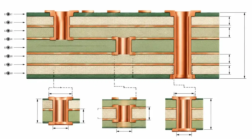
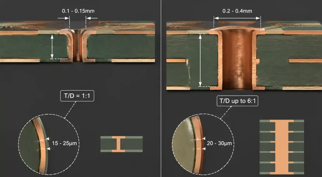
Laser drilling uses CO2 or UV lasers to ablate dielectric material. It’s the standard for microvias in HDI boards—1+N+1 and 2+N+2 stackups. Minimum hole size: 0.1–0.15mm (4–6 mils). Laser gives you small, precise holes with no mechanical stress, which means tighter T/D ratios and finer BGA pitch support.
Mechanical drilling uses carbide drill bits at 80,000–150,000 RPM. It’s the conventional method for through-hole and larger blind/buried vias. Minimum diameter: 0.15–0.2mm (6–8 mils), depending on board thickness. Mechanical handles deeper holes better than laser—if your blind via spans multiple layers, mechanical is often the only option.
T/D Ratio Design Rules and Manufacturing Capabilities
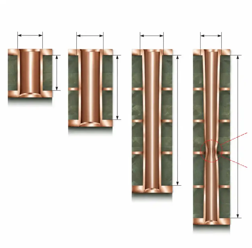
The T/D ratio controls via manufacturability. Higher ratio = deeper, narrower hole = harder to plate = more void risk.
| Drilling Method | Typical Diameter Range | Max T/D (Class 2) | Max T/D (Class 3) | Best For |
|---|---|---|---|---|
| Laser (CO2/UV) | 0.1–0.15mm (4–6 mils) | 1.2:1 | 1:1 | HDI microvias, fine-pitch BGA |
| Mechanical (small) | 0.15–0.3mm (6–12 mils) | 4:1 | 3:1 | Multi-layer blind vias |
| Mechanical (standard) | 0.3–0.6mm (12–24 mils) | 8:1 | 6:1 | Deep blind vias, standard multilayer |
For laser microvias, the safe limit is 1:1 for Class 3, 1.2:1 for Class 2. Some shops push to 1.5:1 with specialized processes, but that adds cost and lead time. For mechanically drilled blind vias, 3:1 to 4:1 is typical for small diameters (0.2–0.3mm), while larger diameters (0.4–0.6mm) can hit 6:1 to 8:1. But plating uniformity gets tricky above 6:1—the center of the barrel tends to plate thin.
T/D Ratio and Reliability
High T/D ratios cause three problems: plating voids, which open up after thermal cycling; poor copper distribution in the barrel center; and via stub effects that mess with signal integrity above 10 Gbps.
For automotive and industrial applications, IPC Class 3 requires conservative T/D ratios because thermal cycling from -40°C to +125°C will find any void. For high-speed digital (DDR4/5, PCIe Gen 4/5, USB 3.2/4.0), laser microvias with low T/D ratios give you shorter stubs and cleaner signals. Designs requiring HDI PCB with mSAP process can push trace geometries to 25/25μm, but via aspect ratios still need to stay within manufacturable limits—mSAP doesn’t magically fix a 2:1 laser via.
DFM Guidelines
| Design Parameter | Recommended Rule | Risk if Violated | Fix |
|---|---|---|---|
| Laser microvia T/D | ≤1:1 (Class 3), ≤1.2:1 (Class 2) | Plating voids, opens after reflow | Thinner core or larger via |
| Mechanical blind via T/D | ≤6:1 (Class 3), ≤8:1 (Class 2) | Poor plating, barrel cracks | Fewer layers or larger diameter |
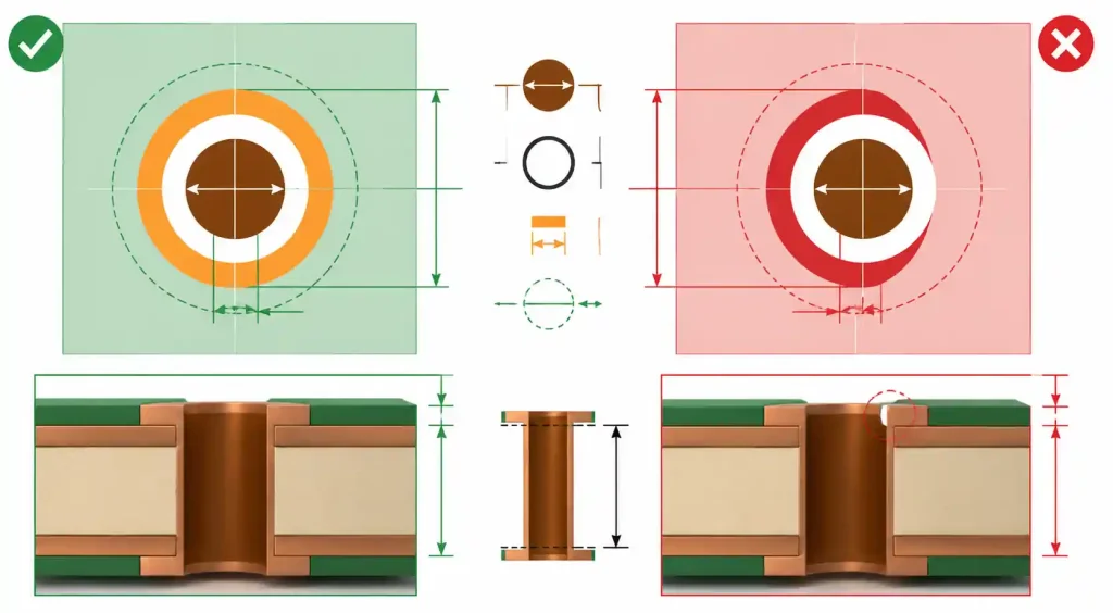
| Capture pad size | Via dia + 0.1mm min | Insufficient annular ring | Larger pad or via-in-pad |
| Blind via-to-trace clearance | ≥0.1mm (4 mils) | Shorts, CAM issues | Increase clearance |
| Staggered via offset | ≥0.3mm between layers | Warpage, lamination voids | Stagger, don’t stack |
Stacked microvias are a common trouble spot. Some shops support them, but stacking increases lamination void risk and Z-axis expansion mismatch. If you need vertical transitions, use filled and capped microvias or staggered placement.
Annular ring is another gotcha. Registration tolerance is typically ±0.075–0.1mm. If your pad is too small, the drill breaks out after registration shift. For Class 3, minimum annular ring is 0.05mm (2 mils) after tolerance—that usually means pad diameter = via diameter + 0.15mm or more.
Decision Framework: Laser vs Mechanical
Choose laser when:
- Via depth ≤0.15mm (single prepreg layer)
- Hole diameter 0.1–0.15mm
- Fine-pitch BGA (0.4mm, 0.5mm pitch)
- High-speed signals where stub length matters
- You’re using sequential lamination (HDI process)
Choose mechanical when:
- Via depth >0.2mm (multiple layers)
- Hole diameter ≥0.2mm
- T/D ratio >1.5:1
- You want lower cost for moderate-density designs
- Conventional multilayer stackup (non-HDI)
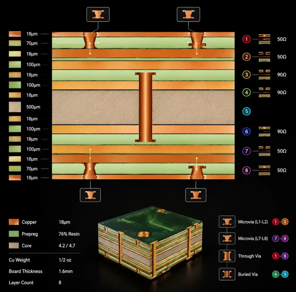
You can mix both methods in hybrid designs: laser for outer-layer-to-inner-layer microvias, mechanical for deeper layer transitions. Common in 10+ layer boards with mixed signal types. For boards that combine HDI routing with flexible sections, the 3+N+3 HDI flex structure introduces additional via placement constraints—keep microvias at least 3mm from bend lines and use staggered (not stacked) vias in flex zones to avoid barrel cracking during dynamic flexing.
FAQ
What’s the maximum T/D ratio for laser-drilled microvias?
1:1 for Class 3, 1.2:1 for Class 2. Some shops push to 1.5:1 with specialized processes, but that adds cost. Stay at or below 1:1 for reliable plating and good yield.
Can I mechanically drill 0.1mm blind vias?
Technically yes, but not practical for production—drill bits break, cost goes up. Laser drilling is standard for diameters below 0.15mm. For 0.15–0.2mm, mechanical becomes feasible but laser is still preferred for shallow depths.
How does T/D ratio affect plating thickness?
Higher ratios make uniform copper plating harder. The center of the via barrel (“knee”) plates thinner than the ends. Above 8:1, center thickness can drop below IPC-6012 Class 2 minimums (18μm). This is why Class 3 designs limit T/D more strictly.
What’s the difference between stacked and staggered microvias?
Stacked = vertically aligned through multiple layers. Staggered = offset by at least 0.3mm between layers. Stacked saves space but increases void and CTE mismatch risk. Staggered is more reliable but uses more board area. For Class 3, staggered is recommended.
How do I calculate minimum capture pad size?
Min pad diameter = via diameter + (2 × min annular ring) + (2 × registration tolerance). Class 2: annular ring 0.05mm, registration ±0.075mm → for 0.2mm via, min pad = 0.2 + 0.1 + 0.15 = 0.45mm. Class 3: 0.075mm annular ring → 0.5mm pad.
Conclusion
T/D ratio control is simple but critical. For laser microvias, keep it at or below 1:1 for Class 3 reliability. For mechanically drilled blind vias, 6:1 (Class 3) or 8:1 (Class 2) is the practical limit—beyond that, plating uniformity falls off and reliability suffers.
Before you submit: verify T/D ratios against your manufacturer’s capability table. For Class 3, stay conservative. For high-speed designs, minimize T/D to reduce stub length. And if you’re using via-in-pad, plan for filled vias—they eliminate air gaps and improve reliability.
If you’re unsure about your stackup or via design, run it past your PCB manufacturer’s CAM team before finalizing. They’ve seen the mistakes before and can save you a respin.