Usb 2.0 high speed pcb layout
A USB 2.0 high-speed PCB layout typically consists of several layers of copper traces and vias that connect various components and ICs…
A USB 2.0 high-speed PCB layout typically consists of several layers of copper traces and vias that connect various components and ICs…

High-speed PCB traces are used in electronic circuits to transmit signals at high frequencies, typically above 50 MHz.These traces are…
High-speed RF PCB design refers to the process of designing printed circuit boards that are optimized for high-frequency signals,typically in…
1. Vector Institute: This institute offers a course on high speed PCB design using Altium Designer software. The course covers…
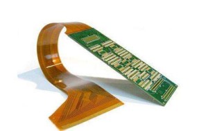
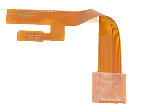
Flex PCB strain relief is a technique used to prevent mechanical stress or strain on the flexible printed circuit board (PCB) during…
1. Flex Ltd.2. Jabil Inc.3. Sanmina Corporation4. TTM Technologies5. Multek Corporation6. Advanced Circuits7. Sierra Circuits8. All Flex Inc.9. Epec Engineered…

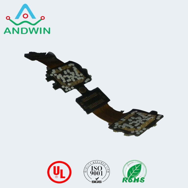
In the ever-evolving world of electronics, the demand for smaller, lighter, and more flexible devices continues to grow. This has…

1. Differential pair routing: This involves routing two signals that are equal in magnitude and opposite in polarity,which helps to…
A high speed PCB drilling machine is a specialized tool used for drilling small holes in printed circuit boards (PCBs).These…
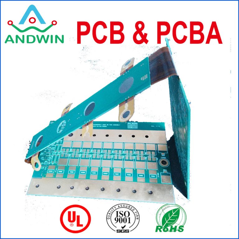
Rigid flex PCBs, a combination of rigid and flexible printed circuit boards, have gained immense popularity in various industries due…
In the world of electronic design, there are numerous factors to consider when selecting the right materials and components for…
There are many sources for high speed signal PCB design, including: 1. Altium Designer: A popular PCB design software that…
High-speed PCB design with EMI resilience is a critical aspect of electronic product development. 1. Grounding and shielding: Proper grounding…

High speed interfaces in PCB (Printed Circuit Board) refer to the communication links between electronic components that operate at high…
High speed PCB design refers to the process of designing printed circuit boards that can handle high frequency signals without…
We use cookies to improve your experience on our site. By using our site, you consent to cookies.
Manage your cookie preferences below:
Essential cookies enable basic functions and are necessary for the proper function of the website.
Statistics cookies collect information anonymously. This information helps us understand how visitors use our website.
Google Analytics is a powerful tool that tracks and analyzes website traffic for informed marketing decisions.
Service URL: policies.google.com (opens in a new window)
SourceBuster is used by WooCommerce for order attribution based on user source.
You can find more information in our privacy policy and privacy policy.