
Skip to content
Andwin Circuits
  • Home
  • ProductsExpand
    • HDI multilayer PCB
    • Rigid Flex PCB
    • Flex pcb
    • Special PCBExpand
      • High Frequency PCBExpand
        • Rogers RO4350B PCB
        • Rogers RO4003 pcb
        • Rogers RO3003 PCB
        • Rogers 5880 PCB
        • DICLAD 527 PCB
        • Taconic TLX series
        • Taconic TLX-8 RF PCB
        • Taconic TLX-9 RF PCB
      • High speed pcbExpand
        • Megtron 6 High Speed PCB
        • TU-872 SLK Sp High Speed
      • High TG PCBExpand
        • SHENGYI SH260 PCB
        • ISOLA 370HR PCB
        • ISOLA IS410 PCB
        • ISOLA IS420 PCB
      • Heavy copper PCB
      • Copper coin pcb
      • Copper inlay PCB
    • Metal Core PCBExpand
      • Copper core pcb
      • Aluminum PCB
      • 2 Layers Aluminum PCB
      • Direct thermal MCPCB
      • 2 Layers Direct Thermal
    • Ceramic PCBExpand
      • DPC ceramic PCB
      • DBC ceramic PCB
      • Thick film Ceramic PCB
      • Al2O3 Alumina PCB
      • AIN ALN ceramic PCB
      • IGBT Ceramic PCB
  • ServiceExpand
    • PCB Assembly
    • Quick turn PCB assembly
    • PCBA conformal coating
  • IndustryExpand
    • Telecommunication
    • IoT and Wireless
    • Industrial Control
    • Thermal management
    • Power and Energy
    • IC test board
    • Automative
    • Medical
  • CapabilityExpand
    • Rigid PCB
    • Rigid flex PCB
    • Metal core PCB
    • PCB Assembly
  • TechnologyExpand
    • Blogs
    • Via in pad
    • PCB E-test
    • PCB stack up
    • MCPCB panelization
    • Controlled impedance PCB
  • AboutExpand
    • About us
    • Certification
    • Factory Tour
  • Contact
Andwin Circuits
Home / Briefly describe the functions of each layer in the PCB board and the precautions during use

Briefly describe the functions of each layer in the PCB board and the precautions during use

ByGrace February 25, 2025February 24, 2025

Many PCB board design enthusiasts, especially beginners, do not have a full understanding of the various layers in PCB design, and do not know their functions and uses. Here is a systematic explanation for everyone:

1.Mechanical mechanical layer, as the name implies, is the appearance of the entire PCB board for mechanical shaping.

In fact, when we talk about mechanical layer, we refer to the appearance structure of the entire PCB board. It can also be used to set the board’s external dimensions, data marks, alignment marks, assembly instructions and other mechanical information. This information varies depending on the requirements of the design company or PCB manufacturer. In addition, the mechanical layer can be attached to other layers for output display.

2.Keep out layer (forbidden wiring layer), used to define the area on the circuit board where components and wiring can be effectively placed.

Draw a closed area on this layer as the wiring effective area, and automatic layout and wiring cannot be performed outside this area. The keepout layer is used to define the boundary of the copper with electrical characteristics when we lay it. That is to say, after we define the keepout layer, the wires with electrical characteristics laid in the subsequent laying process cannot exceed the boundary of the keepout layer. It is often customary to use the keepout layer as a mechanical layer. This method is actually wrong, so it is recommended that you distinguish it, otherwise the board factory will change the attributes for you every time you produce it.
Contact us for PCB quote now |

3.Signal layer:

The signal layer is mainly used to arrange the wires on the circuit board. Including Top layer, Bottom layer and 30 MidLayers. The top and bottom layers are used to place devices, and the inner layers are used for routing.

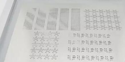
4.Top paste and Bottom paste are the top and bottom pad steel mesh layers, which are the same size as the pad.

This is mainly because we can use these two layers to make steel mesh when doing SMT. We just dig a hole the size of the pad on the steel mesh, and then we cover the steel mesh on the PCB board. We use a brush with solder paste to evenly apply solder paste, as shown in Figure 2-1.
5.Top Solder and Bottom Solder This is the solder mask layer, which prevents green oil from covering, which we often call “opening a window”.

Conventional copper plating or routing is covered with green oil by default. If we process it in the solder mask layer accordingly, it will prevent green oil from covering and expose the copper. The difference between the two can be seen in the following figure:

6.Internal plane layer (internal power/ground layer):

This type of layer is only used for multi-layer boards, mainly for arranging power lines and ground lines. We call it double-layer board, four-layer board, six-layer board, generally referring to the number of signal layers and internal power/ground layers.

7.Silkscreen layer:

The silkscreen layer is mainly used to place printed information, such as the outline and annotation of components, various annotation characters, etc. Altium provides two silkscreen layers, Top Overlay and Bottom Overlay, to place the top silkscreen file and the bottom silkscreen file respectively.

8.Multi layer:

The pads and through-holes on the circuit board need to penetrate the entire circuit board and establish electrical connections with different conductive graphic layers. Therefore, the system specifically sets up an abstract layer – multilayer. Generally, pads and vias must be set on multiple layers. If this layer is closed, the pads and vias cannot be displayed.

9.Drill Drawing:

The drilling layer provides drilling information during the circuit board manufacturing process (such as pads and vias need to be drilled). Altium provides two drilling layers, Drill gride (drilling indication diagram) and Drill drawing (drilling diagram).

    Contact us for PCB quote now |
    Post Tags: #aluminum clad pcb#aluminum core pcb#aluminum core pcb led#aluminum pcb#assemble pcb

    Post navigation

    Previous Previous
    Source of circuit board
    NextContinue
    Summary of circuit board failures and several tricks for repair technology

    Search

    Search

    Products

    • HDI Multilayer PCB
    • Rigid Flex PCB
    • Flex pcb
    • High Frequency PCB
    • High speed pcb
    • Heavy copper PCB
    • Metal Core PCB
    • Ceramic PCB

    Address

    Andwin Circuits Co.,Limited
    Email: sales@andwinpcb.com
    Tel: +86 755 2832 9394
    Fax:+86 755 2992  6717
    ADD:1-2F-1217,HouDeQun Industrial park,
    NanTing RD NO.56,ShaJing,BaoAn,Shenzhen 518104,GuangDong,China

    Products

    • HDI Multilayer PCB
    • Rigid Flex PCB
    • Flex pcb
    • High Frequency PCB
    • High speed pcb
    • Heavy copper PCB
    • Metal Core PCB
    • Ceramic PCB

    Technology

    • Blogs
    • Via in pad
    • PCB E-test
    • PCB stack up
    • Metal core PCB panelization
    • Controlled impedance PCB

    CERTIFICATION

    Certification >>


    Copyright© 2003 - 2026 Andwin | All Rights Reserved | Powered by Andwin

    Scroll to top
    • Home
    • Products
      • HDI multilayer PCB
      • Rigid Flex PCB
      • Flex pcb
      • Special PCB
        • High Frequency PCB
          • Rogers RO4350B PCB
          • Rogers RO4003 pcb
          • Rogers RO3003 PCB
          • Rogers 5880 PCB
          • DICLAD 527 PCB
          • Taconic TLX series
          • Taconic TLX-8 RF PCB
          • Taconic TLX-9 RF PCB
        • High speed pcb
          • Megtron 6 High Speed PCB
          • TU-872 SLK Sp High Speed
        • High TG PCB
          • SHENGYI SH260 PCB
          • ISOLA 370HR PCB
          • ISOLA IS410 PCB
          • ISOLA IS420 PCB
        • Heavy copper PCB
        • Copper coin pcb
        • Copper inlay PCB
      • Metal Core PCB
        • Copper core pcb
        • Aluminum PCB
        • 2 Layers Aluminum PCB
        • Direct thermal MCPCB
        • 2 Layers Direct Thermal
      • Ceramic PCB
        • DPC ceramic PCB
        • DBC ceramic PCB
        • Thick film Ceramic PCB
        • Al2O3 Alumina PCB
        • AIN ALN ceramic PCB
        • IGBT Ceramic PCB
    • Service
      • PCB Assembly
      • Quick turn PCB assembly
      • PCBA conformal coating
    • Industry
      • Telecommunication
      • IoT and Wireless
      • Industrial Control
      • Thermal management
      • Power and Energy
      • IC test board
      • Automative
      • Medical
    • Capability
      • Rigid PCB
      • Rigid flex PCB
      • Metal core PCB
      • PCB Assembly
    • Technology
      • Blogs
      • Via in pad
      • PCB E-test
      • PCB stack up
      • MCPCB panelization
      • Controlled impedance PCB
    • About
      • About us
      • Certification
      • Factory Tour
    • Contact
    Search