additive pcb manufacturing | advanced assembly pcb | advanced circuit board | advanced circuits 4pcb | advanced circuits assembly | advanced circuits barebones | advanced circuits flex pcb | advanced circuits pcb | advanced circuits pcb artist | advanced circuits quote | advanced pcb manufacturing | advanced printed circuit technology
The Role and Techniques of Copper Cladding in PCB Design
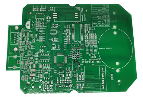
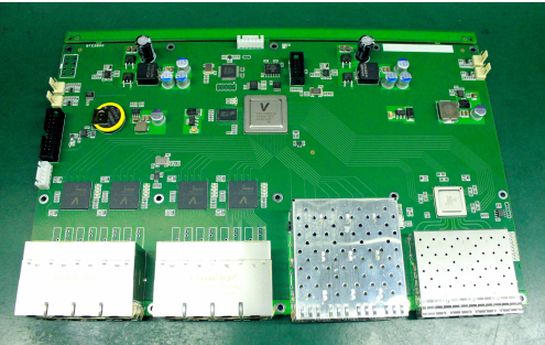
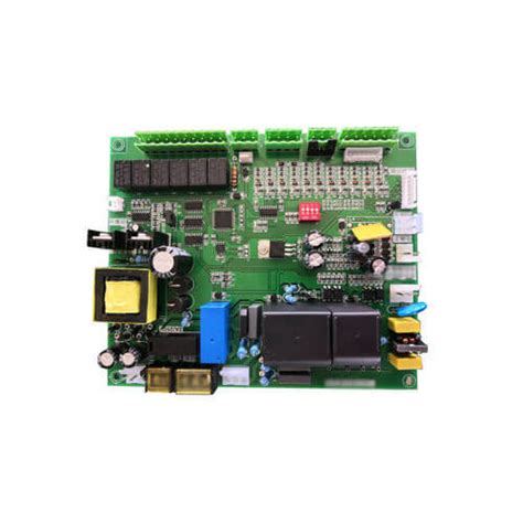
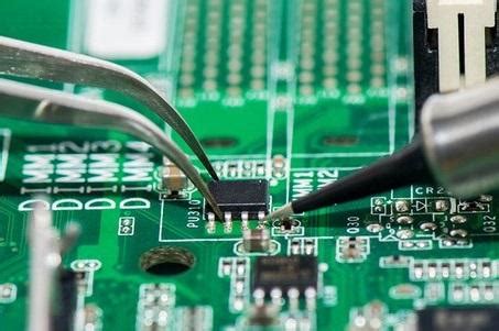
Introduction Copper cladding, also known as copper pour or copper fill, is a fundamental aspect of Printed Circuit Board (PCB) design. It involves the strategic placement of copper areas on the PCB to enhance electrical performance, thermal management, and mechanical stability. This article delves into the significance of copper cladding, its various techniques, and best…