advanced circuits barebones | advanced circuits pcb | advanced circuits pcb artist | advanced circuits quote | all flex pcb | altium multi board assembly | altium multiboard assembly | alumina pcb manufacturer | Aluminum PCB | uncategories
What is the significance of each layer in PCB design?
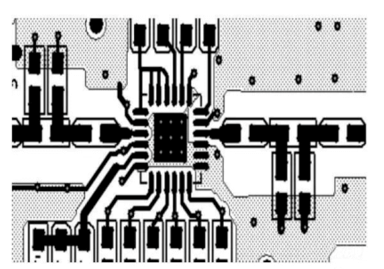
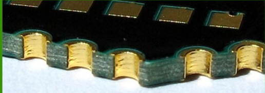
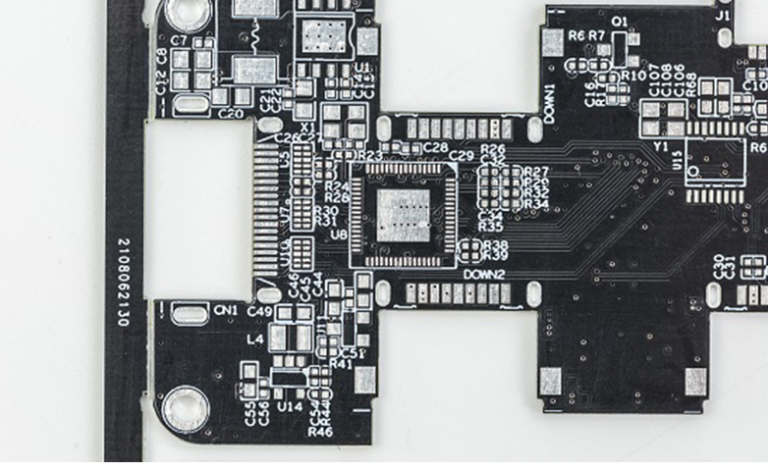
1.Signal layers Altium Designer can provide up to 32 signal layers,including the top layer,bottom layer,and mid-layer.Each layer can be connected to each other through via,blind vias,and buries vias. (1)Top signal Layer Also known as the component layer,it is mainly uesd to place components.For double-layer and multi-layer boards,it can be used to arrange wires or copper….