
Designing RF Circuits and PCB Layout: A Comprehensive Guide
Introduction
Radio Frequency (RF) circuit design and PCB layout are critical aspects of modern wireless communication systems, including Wi-Fi, Bluetooth, cellular networks, and IoT devices. Designing an efficient RF circuit requires careful consideration of signal integrity, impedance matching, noise reduction, and electromagnetic interference (EMI). Additionally, PCB layout plays a crucial role in ensuring optimal performance, as poor layout practices can degrade signal quality and introduce unwanted noise.
This article provides a detailed guide on designing RF circuits and their PCB layouts, covering key principles, best practices, and common challenges.
1. Fundamentals of RF Circuit Design
1.1 Understanding RF Signals
RF signals operate at high frequencies (typically from 30 MHz to several GHz), where wavelength becomes comparable to the physical dimensions of PCB traces. At these frequencies, transmission line effects such as reflections, standing waves, and parasitic capacitance/inductance become significant.
1.2 Key Parameters in RF Design
- Frequency Range: Determines the choice of components and transmission line design.
- Impedance Matching: Ensures maximum power transfer (typically 50Ω in RF systems).
- Insertion Loss & Return Loss: Measures signal attenuation and reflections.
- Noise Figure (NF): Indicates signal degradation due to noise.
- Gain & Linearity: Important for amplifiers to avoid distortion.
1.3 RF Components
- Active Components: RF amplifiers, mixers, oscillators, and transceivers.
- Passive Components: Resistors, capacitors, inductors, and filters optimized for high-frequency operation.
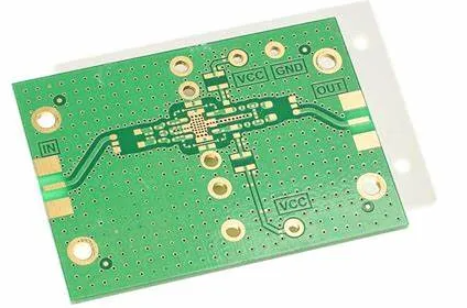
- Transmission Lines: Microstrip, stripline, and coplanar waveguide (CPW) structures.
2. RF PCB Layout Considerations
2.1 Material Selection
- Substrate Material: FR4 is common but has high loss at RF frequencies. High-frequency laminates like Rogers RO4003C or Teflon are preferred for GHz applications.
- Dielectric Constant (Dk): Affects impedance and signal propagation speed.
- Loss Tangent (Df): Determines signal attenuation; lower values are better.
2.2 Layer Stackup
- Multilayer PCBs: Provide better EMI shielding and ground planes.
- Ground Planes: Essential for reducing noise and maintaining consistent impedance.
- Signal Layer Separation: High-frequency signals should be routed on inner layers to minimize radiation.
2.3 Transmission Line Design
- Microstrip Lines: A conductor on top of a dielectric with a ground plane beneath.
- Stripline: A conductor embedded between two ground planes for better shielding.
- Coplanar Waveguide (CPW): A conductor with adjacent ground planes on the same layer.
Impedance Calculation: Tools like ADS, HFSS, or online calculators help determine trace width and spacing for desired impedance (e.g., 50Ω).
2.4 Grounding Techniques
- Solid Ground Plane: Minimizes loop inductance and EMI.
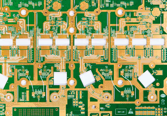
- Via Stitching: Multiple vias connect ground layers to reduce impedance discontinuities.
- Ground Isolation: Separate analog, digital, and RF grounds to avoid noise coupling.
2.5 Component Placement
- Short RF Traces: Minimize parasitic inductance and capacitance.
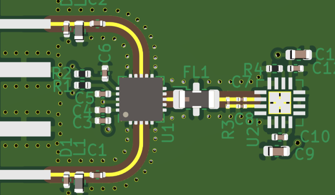
- Decoupling Capacitors: Place close to ICs to suppress high-frequency noise.
- Isolation of Sensitive Components: Keep oscillators and amplifiers away from noisy digital circuits.
2.6 Shielding & EMI Reduction
- RF Shielding Cans: Used to block external interference.
- Guard Traces: Grounded traces around RF signals to prevent crosstalk.
- Avoiding Sharp Corners: Use curved or 45° bends to reduce reflections.
3. Common Challenges & Solutions
3.1 Parasitic Effects
- Parasitic Capacitance/Inductance: Minimized by using surface-mount components and short traces.
- Skin Effect: At high frequencies, current flows near the conductor surface, increasing resistance. Use wider traces or gold plating.
3.2 Crosstalk & Interference
- Adequate Spacing: Maintain distance between RF and digital traces.
- Differential Signaling: Reduces noise susceptibility in high-speed RF lines.
3.3 Thermal Management
- Thermal Vias: Dissipate heat from power amplifiers.
- Copper Pours: Improve heat dissipation for high-power components.
3.4 Manufacturing Tolerances
- Controlled Impedance Fabrication: Work with PCB manufacturers to ensure precise trace dimensions.
- Tuning & Testing: Post-layout adjustments may be needed for optimal performance.
4. Simulation & Testing
4.1 Simulation Tools
- SPICE-based Tools (LTspice, PSpice): For basic circuit analysis.
- EM Simulators (HFSS, CST, ADS): For full-wave RF analysis.
- Impedance Calculators (Polar SI9000): For transmission line design.
4.2 Testing & Validation
- Network Analyzer: Measures S-parameters (S11, S21) for impedance matching.
- Spectrum Analyzer: Checks for spurious emissions and noise.
- Oscilloscope: Verifies signal integrity in time domain.
5. Best Practices Summary
- Keep RF traces short and direct to minimize losses.
- Use proper impedance matching (50Ω standard for most RF systems).
- Implement strong grounding techniques to reduce noise.
- Shield sensitive components from digital noise.
- Simulate before fabrication to avoid costly redesigns.
- Test thoroughly with RF measurement equipment.
Conclusion
Designing RF circuits and their PCB layouts requires a deep understanding of high-frequency signal behavior, material properties, and EMI mitigation techniques. By following best practices in component selection, transmission line design, grounding, and shielding, engineers can achieve optimal RF performance. Simulation and testing play a crucial role in validating designs before manufacturing, ensuring reliability in real-world applications.
With the increasing demand for wireless technologies, mastering RF PCB design is essential for engineers working in telecommunications, IoT, and embedded systems. Continuous learning and staying updated with advanced RF techniques will further enhance design efficiency and performance.