
Skip to content
Andwin Circuits
  • Home
  • ProductsExpand
    • HDI multilayer PCB
    • Rigid Flex PCB
    • Flex pcb
    • Special PCBExpand
      • High Frequency PCBExpand
        • Rogers RO4350B PCB
        • Rogers RO4003 pcb
        • Rogers RO3003 PCB
        • Rogers 5880 PCB
        • DICLAD 527 PCB
        • Taconic TLX series
        • Taconic TLX-8 RF PCB
        • Taconic TLX-9 RF PCB
      • High speed pcbExpand
        • Megtron 6 High Speed PCB
        • TU-872 SLK Sp High Speed
      • High TG PCBExpand
        • SHENGYI SH260 PCB
        • ISOLA 370HR PCB
        • ISOLA IS410 PCB
        • ISOLA IS420 PCB
      • Heavy copper PCB
      • Copper coin pcb
      • Copper inlay PCB
    • Metal Core PCBExpand
      • Copper core pcb
      • Aluminum PCB
      • 2 Layers Aluminum PCB
      • Direct thermal MCPCB
      • 2 Layers Direct Thermal
    • Ceramic PCBExpand
      • DPC ceramic PCB
      • DBC ceramic PCB
      • Thick film Ceramic PCB
      • Al2O3 Alumina PCB
      • AIN ALN ceramic PCB
      • IGBT Ceramic PCB
  • ServiceExpand
    • PCB Assembly
    • Quick turn PCB assembly
    • PCBA conformal coating
  • IndustryExpand
    • Telecommunication
    • IoT and Wireless
    • Industrial Control
    • Thermal management
    • Power and Energy
    • IC test board
    • Automative
    • Medical
  • CapabilityExpand
    • Rigid PCB
    • Rigid flex PCB
    • Metal core PCB
    • PCB Assembly
  • TechnologyExpand
    • Blogs
    • Via in pad
    • PCB E-test
    • PCB stack up
    • MCPCB panelization
    • Controlled impedance PCB
  • AboutExpand
    • About us
    • Certification
    • Factory Tour
  • Contact
Andwin Circuits
Home / Blogs / Electrical and Non-Electrical Safety Spacing in PCB Design

Electrical and Non-Electrical Safety Spacing in PCB Design

ByGrace May 22, 2025May 21, 2025

Abstract

Printed Circuit Board (PCB) design involves numerous critical considerations to ensure functionality, reliability, and safety. Among these, maintaining appropriate safety spacing—both electrical and non-electrical—is paramount. Electrical spacing pertains to clearance and creepage distances to prevent short circuits and voltage breakdown, while non-electrical spacing involves mechanical, thermal, and manufacturing constraints. This paper explores the key aspects of safety spacing in PCB design, including industry standards, design guidelines, and practical implementation strategies.

1. Introduction

PCB design requires meticulous attention to spacing rules to avoid electrical failures, signal interference, and manufacturing defects. Safety spacing can be broadly categorized into:

  • Electrical Spacing: Minimum distances to prevent arcing, leakage, and short circuits.
  • Non-Electrical Spacing: Mechanical, thermal, and assembly-related clearances.

Understanding and implementing these spacing rules ensures compliance with safety standards such as IPC (Association of Connecting Electronics Industries), UL (Underwriters Laboratories), and IEC (International Electrotechnical Commission).
2. Electrical Safety Spacing

2.1 Clearance and Creepage

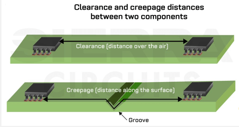
  • Clearance (Air Gap): The shortest distance between two conductive elements through air. High-voltage applications require larger clearances to prevent arcing.
  • Creepage Distance: The shortest path along the surface of insulation between conductors. Contamination (dust, moisture) can reduce effective creepage, necessitating greater spacing.

Factors Influencing Electrical Spacing:

  • Voltage Levels: Higher voltages require larger clearances (e.g., IPC-2221 specifies 0.1mm per 10V for low-voltage boards).
  • Environmental Conditions: Humidity, pollution, and altitude affect dielectric strength.
  • Material Properties: PCB substrate (FR-4, polyimide) impacts insulation resistance.

2.2 High-Voltage Design Considerations

For high-voltage PCBs (e.g., power supplies, industrial equipment):

  • Increased Clearance: Follow IEC 60950-1 or IPC-2221 standards.
  • Slotting and Grooving: Used to extend creepage paths in constrained layouts.
  • Conformal Coating: Provides additional insulation in harsh environments.

2.3 Signal Integrity and EMI Mitigation

  • Trace Spacing: High-speed signals require controlled impedance and spacing to prevent crosstalk (e.g., 3W rule: spacing ≥ 3x trace width).
  • Ground Planes: Proper grounding reduces electromagnetic interference (EMI).
Contact us for PCB quote now |

3. Non-Electrical Safety Spacing

3.1 Mechanical and Assembly Constraints

  • Component Placement: Adequate spacing prevents physical interference during assembly (e.g., SMD reflow soldering requires clearance for pick-and-place machines).
  • Edge Clearance: Components should be placed at least 3-5mm from board edges to avoid damage during panelization.

3.2 Thermal Management

  • Heat-Generating Components (e.g., MOSFETs, regulators): Increased spacing improves airflow and heat dissipation.
  • Thermal Relief Pads: Used in high-current traces to prevent solder wicking.

3.3 Manufacturing Tolerances

  • Drill-to-Copper Distance: Minimum spacing (typically 0.2mm) prevents breakout in drilled holes.
  • Solder Mask Clearance: Ensures proper solder application and prevents bridging.

4. Industry Standards and Compliance

  • IPC-2221: Generic standard for PCB design, covering electrical and mechanical spacing.
  • IPC-7351: Guidelines for land pattern and component spacing.
  • IEC 60664: Insulation coordination for high-voltage equipment.
  • UL 60950-1: Safety requirements for IT equipment.

5. Best Practices for PCB Layout

  1. Use Design Rule Checks (DRC): Automated tools in CAD software (e.g., Altium, KiCad) enforce spacing rules.
  2. Simulate High-Voltage Conditions: Verify clearance and creepage using field solvers.
  3. Optimize Layer Stackup: Proper grounding and shielding reduce EMI.
  4. Review Manufacturer Capabilities: Ensure design aligns with fabrication tolerances.

6. Conclusion

Safety spacing in PCB design is crucial for electrical reliability, manufacturability, and compliance with industry standards. Electrical spacing prevents short circuits and voltage breakdown, while non-electrical spacing ensures mechanical robustness and thermal efficiency. By adhering to established guidelines and leveraging modern design tools, engineers can develop high-performance PCBs that meet safety and functional requirements.

Contact us for PCB quote now |
Post Tags: #aluminum clad pcb#aluminum core pcb#aluminum pcb#assemble pcb#Electrical and Non-Electrical Safety Spacing in PCB Design

Post navigation

Previous Previous
Causes and Solutions for PCB Overheating
NextContinue
The Correct Placement of Inductors in PCB Design for Switch-Mode Power Supplies

Search

Search

Products

  • HDI Multilayer PCB
  • Rigid Flex PCB
  • Flex pcb
  • High Frequency PCB
  • High speed pcb
  • Heavy copper PCB
  • Metal Core PCB
  • Ceramic PCB

Address

Andwin Circuits Co.,Limited
Email: sales@andwinpcb.com
Tel: +86 755 2832 9394
Fax:+86 755 2992  6717
ADD:1-2F-1217,HouDeQun Industrial park,
NanTing RD NO.56,ShaJing,BaoAn,Shenzhen 518104,GuangDong,China

Products

  • HDI Multilayer PCB
  • Rigid Flex PCB
  • Flex pcb
  • High Frequency PCB
  • High speed pcb
  • Heavy copper PCB
  • Metal Core PCB
  • Ceramic PCB

Technology

  • Blogs
  • Via in pad
  • PCB E-test
  • PCB stack up
  • Metal core PCB panelization
  • Controlled impedance PCB

CERTIFICATION

Certification >>


Copyright© 2003 - 2026 Andwin | All Rights Reserved | Powered by Andwin

Scroll to top
  • Home
  • Products
    • HDI multilayer PCB
    • Rigid Flex PCB
    • Flex pcb
    • Special PCB
      • High Frequency PCB
        • Rogers RO4350B PCB
        • Rogers RO4003 pcb
        • Rogers RO3003 PCB
        • Rogers 5880 PCB
        • DICLAD 527 PCB
        • Taconic TLX series
        • Taconic TLX-8 RF PCB
        • Taconic TLX-9 RF PCB
      • High speed pcb
        • Megtron 6 High Speed PCB
        • TU-872 SLK Sp High Speed
      • High TG PCB
        • SHENGYI SH260 PCB
        • ISOLA 370HR PCB
        • ISOLA IS410 PCB
        • ISOLA IS420 PCB
      • Heavy copper PCB
      • Copper coin pcb
      • Copper inlay PCB
    • Metal Core PCB
      • Copper core pcb
      • Aluminum PCB
      • 2 Layers Aluminum PCB
      • Direct thermal MCPCB
      • 2 Layers Direct Thermal
    • Ceramic PCB
      • DPC ceramic PCB
      • DBC ceramic PCB
      • Thick film Ceramic PCB
      • Al2O3 Alumina PCB
      • AIN ALN ceramic PCB
      • IGBT Ceramic PCB
  • Service
    • PCB Assembly
    • Quick turn PCB assembly
    • PCBA conformal coating
  • Industry
    • Telecommunication
    • IoT and Wireless
    • Industrial Control
    • Thermal management
    • Power and Energy
    • IC test board
    • Automative
    • Medical
  • Capability
    • Rigid PCB
    • Rigid flex PCB
    • Metal core PCB
    • PCB Assembly
  • Technology
    • Blogs
    • Via in pad
    • PCB E-test
    • PCB stack up
    • MCPCB panelization
    • Controlled impedance PCB
  • About
    • About us
    • Certification
    • Factory Tour
  • Contact
Search