
Halogen-Free PCB: Materials, Standards, and Environmental Benefits
If you want to design electronics that meet modern environmental standards and minimize toxic emissions, then you will need to understand halogen-free PCB technology. Halogen-free printed circuit boards eliminate bromine and chlorine from base materials, reducing toxic gas release during manufacturing and end-of-life disposal while maintaining reliable electrical performance.
In today’s article, we will explain halogen-free PCB materials, the international standards that define them, and why engineers increasingly choose them for consumer electronics, automotive, and medical applications. This guide will help you specify the right materials for your next project while meeting RoHS 3.0 and sustainability requirements.
What Is Halogen-Free PCB?
A halogen-free PCB is a printed circuit board manufactured using laminate materials and substrates that contain minimal chlorine (Cl) and bromine (Br) content. According to IEC 61249-2-21 and JPCA-ES-01-2003 standards, a PCB qualifies as halogen-free when chlorine content is below 900 ppm, bromine content is below 900 ppm, and the combined total of both halogens is below 1500 ppm.
Traditional PCB laminates use brominated flame retardants (BFRs) to achieve UL 94V-0 flammability ratings. These halogenated materials can release toxic and corrosive gases such as hydrogen bromide and dioxins during thermal stress, combustion, or disposal. Halogen-free alternatives use phosphorus-based or nitrogen-based flame retardants that provide comparable fire safety without harmful emissions.
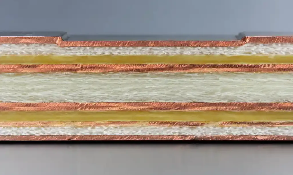
You can specify halogen-free boards for applications where environmental compliance, workplace safety, and reduced toxicity are critical requirements. Industries such as consumer electronics, telecommunications, automotive, and medical devices increasingly adopt halogen-free technology to meet regulatory standards and corporate sustainability goals.
Halogen-Free PCB Materials and Flame Retardant Systems
Phosphorus-Based Flame Retardants
Phosphorus-based systems represent the most common halogen-free flame retardant technology in PCB laminates. These materials work by forming a protective char layer on the substrate surface when exposed to high temperatures, which insulates the underlying material and slows combustion. Red phosphorus and phosphate ester compounds provide effective flame retardancy while maintaining thermal stability up to 170°C Tg.
The phosphorus-nitrogen synergistic system combines both elements to achieve enhanced flame retardant performance. This approach delivers UL 94V-0 ratings comparable to traditional brominated materials while reducing smoke density and toxic gas emissions by up to 60% during thermal decomposition.
Nitrogen-Based Flame Retardants
Nitrogen-containing compounds such as melamine and triazine derivatives function through gas-phase flame inhibition. These materials decompose at elevated temperatures to release non-combustible nitrogen gas, which dilutes oxygen concentration near the flame front and suppresses combustion propagation.
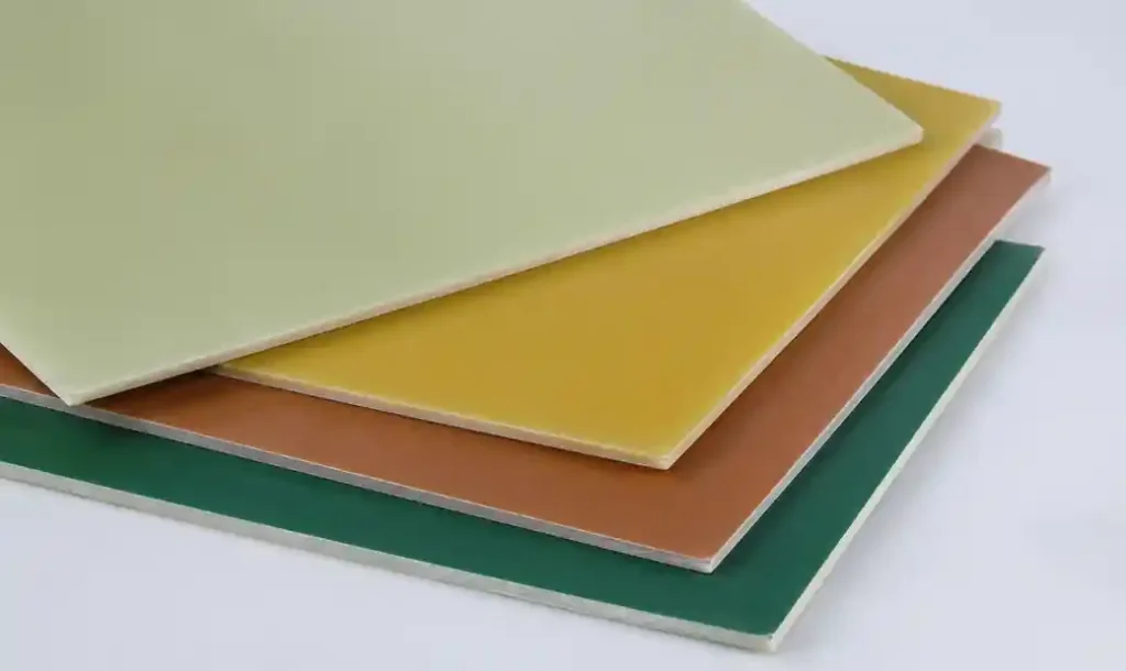
Nitrogen-based systems demonstrate excellent compatibility with high-frequency circuit designs because they maintain stable dielectric constant (Dk) and low dissipation factor (Df) across wide frequency ranges. You can specify these materials for RF applications operating from 1 GHz to 28 GHz where signal integrity is critical.
Metal Hydroxide Fillers
Aluminum hydroxide (ATH) and magnesium hydroxide (MDH) serve as inorganic flame retardants in halogen-free laminates. These metal hydroxides undergo endothermic decomposition when heated, absorbing thermal energy and releasing water vapor that dilutes combustible gases. The process delays ignition and reduces heat release rate without producing toxic emissions.
International Standards for Halogen-Free PCB
| Standard | Chlorine Limit | Bromine Limit | Total Halogen Limit | Region |
|---|---|---|---|---|
| IEC 61249-2-21 | <900 ppm | <900 ppm | <1500 ppm | International |
| JPCA-ES-01-2003 | <900 ppm | <900 ppm | <1500 ppm | Japan |
| iNEMI Definition | <900 ppm | <900 ppm | <1500 ppm | North America/Europe |
| RoHS 3.0 | Regulated | Regulated | Material restrictions | EU |
IEC 61249-2-21 Standard
The International Electrotechnical Commission (IEC) standard IEC 61249-2-21 establishes the globally recognized definition for halogen-free copper-clad laminates. This specification limits individual halogen content to 900 parts per million by weight and total halogens to 1500 ppm. Materials meeting this threshold demonstrate significantly reduced environmental and health risks compared to conventional brominated laminates.
JPCA-ES-01-2003 Standard
The Japan Printed Circuit Association (JPCA) developed JPCA-ES-01-2003 as the first industry standard for halogen-free PCB materials. This specification aligns with IEC 61249-2-21 numerical limits and adds specific test methods for halogen content verification using techniques such as X-ray fluorescence spectroscopy (XRF) and ion chromatography.
RoHS 3.0 Directive Compliance
The European Union’s Restriction of Hazardous Substances (RoHS 3.0) directive regulates specific halogenated flame retardants including polybrominated biphenyls (PBB) and polybrominated diphenyl ethers (PBDE). While RoHS 3.0 does not mandate complete halogen elimination, halogen-free PCBs provide a compliance pathway that exceeds minimum requirements and addresses future regulatory trends.
Environmental Benefits of Halogen-Free PCB
Reduced Toxic Emissions During Manufacturing
Manufacturing processes for halogen-free PCBs generate 40-60% lower levels of corrosive hydrogen halide gases compared to brominated laminates. This reduction improves workplace air quality and minimizes corrosion of production equipment such as reflow ovens, wave soldering systems, and SMT placement machines. Studies show that facilities using halogen-free materials report 30% fewer equipment maintenance requirements related to corrosive damage.
Safer End-of-Life Disposal
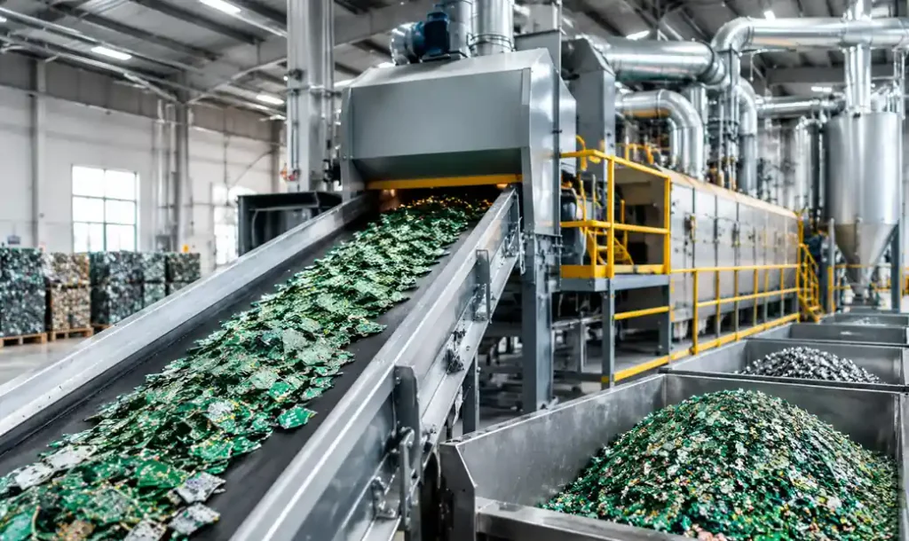
When conventional halogenated PCBs undergo thermal recycling or incineration, they release dioxins, furans, and hydrogen halides that require specialized emission control systems. Halogen-free boards eliminate these hazardous combustion byproducts, simplifying recycling processes and reducing treatment costs. Research indicates that halogen-free PCB incineration produces 86% lower dioxin levels compared to brominated equivalents.
Lower Global Warming Potential
According to lifecycle assessment studies, manufacturing processes using halogen-free laminates can reduce global warming potential (GWP) of PCB production by up to 70-86% when combined with optimized fabrication techniques. The elimination of brominated compounds and associated chemical synthesis steps reduces overall carbon footprint across the production chain.
Improved Workplace Safety
Elimination of halogenated flame retardants reduces occupational exposure to persistent organic pollutants (POPs) and potential carcinogens. Workers in PCB fabrication facilities experience lower health risks from chronic chemical exposure. Halogen-free processing also reduces requirements for specialized ventilation systems and personal protective equipment in manufacturing environments.
Performance Comparison: Halogen-Free vs Traditional PCB
| Parameter | Halogen-Free PCB | Traditional Halogenated PCB |
|---|---|---|
| Flame Retardant | Phosphorus/nitrogen compounds | Brominated flame retardants (BFRs) |
| Tg (Glass Transition) | 150-180°C | 130-180°C |
| Thermal Decomposition | >350°C | >300°C |
| Smoke Density | 40-60% lower | Baseline |
| Toxic Gas Release | Minimal (water vapor, CO₂) | HBr, dioxins, furans |
| Dielectric Constant (1 GHz) | 4.2-4.6 | 4.0-4.5 |
| Lead-Free Compatibility | Excellent (260°C reflow) | Good (260°C reflow) |
| Cost Premium | 5-15% higher | Baseline |
Electrical Performance
Halogen-free laminates using phosphorus-nitrogen flame retardant systems demonstrate electrical properties comparable to standard FR-4 materials. Dielectric constant (Dk) typically ranges from 4.2 to 4.6 at 1 GHz, while dissipation factor (Df) remains below 0.015. You can design controlled impedance circuits with halogen-free materials achieving 50Ω ±5Ω tolerance per IPC-2141 requirements.
Thermal Reliability
Glass transition temperature (Tg) for halogen-free laminates ranges from 150°C to 180°C depending on resin formulation. Higher Tg values ensure dimensional stability during lead-free soldering processes that reach 260°C peak reflow temperature. Thermal decomposition temperature (Td) exceeds 350°C, providing adequate safety margin for standard assembly operations.
Mechanical Properties
Halogen-free substrates maintain flexural strength above 400 MPa and peel strength exceeding 1.4 N/mm per IPC-4101 specifications. These mechanical properties ensure reliable plated through-hole (PTH) integrity and resist delamination during thermal cycling from -40°C to +125°C. You should verify mechanical specifications with your PCB manufacturer for high-reliability applications such as automotive or aerospace.
Applications for Halogen-Free PCB Technology
Consumer Electronics
Smartphones, tablets, laptops, and wearable devices increasingly specify halogen-free PCBs to meet corporate environmental policies and reduce hazardous material content. Major electronics brands including Apple, Samsung, and Sony mandate halogen-free materials for internal components as part of sustainability initiatives.
Automotive Electronics
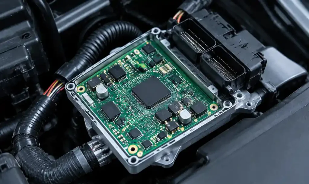
Automotive applications such as ADAS systems, infotainment modules, and battery management systems use halogen-free PCBs to comply with IMDS (International Material Data System) reporting requirements and End-of-Life Vehicles (ELV) directive restrictions. The automotive industry requires halogen-free materials for components that may be exposed to high temperatures near powertrains or in passenger cabin locations.
Telecommunications Infrastructure
5G base stations, network switches, and data center equipment utilize halogen-free PCBs to minimize fire hazards in high-density equipment installations. Telecommunications facilities with thousands of circuit boards benefit from reduced toxic smoke generation in fire scenarios, improving evacuation safety and reducing facility damage.
Medical Devices
Patient monitoring equipment, diagnostic instruments, and implantable device electronics specify halogen-free materials to meet biocompatibility requirements and reduce chemical exposure risks. Medical applications demand materials that minimize off-gassing and maintain stable performance in body-temperature environments from 35°C to 40°C.
Design Considerations for Halogen-Free PCB
Material Selection
Specify halogen-free laminates with Tg values at least 25°C above your maximum operating temperature to ensure dimensional stability. For lead-free assembly processes using SAC305 solder, choose materials with Tg ≥ 150°C to withstand 260°C reflow profiles. Verify that your selected laminate meets IEC 61249-2-21 limits through supplier material data sheets and test certificates.
Lamination Process Adjustment
Halogen-free prepregs may require modified lamination parameters compared to standard FR-4 materials. Typical lamination cycles use temperatures from 180°C to 200°C with press times extended by 10-15% to achieve complete resin cure. Work with your PCB manufacturer to optimize lamination profiles based on specific material properties.
Copper Weight and Trace Design
Halogen-free laminates support copper weights from 0.5 oz to 6 oz (17 μm to 210 μm) depending on laminate thickness and application requirements. You should follow IPC-2221 design rules for minimum trace width and spacing based on copper weight and voltage levels. Heavy copper designs above 3 oz may require special etchback or controlled depth drilling procedures.
Cost Considerations and ROI
Halogen-free PCB materials typically cost 5-15% more than equivalent brominated laminates due to specialized flame retardant formulations and lower production volumes. However, total cost of ownership analysis should include environmental compliance benefits, reduced waste disposal costs, and improved corporate sustainability metrics.
For high-volume consumer electronics production exceeding 100,000 units annually, the material cost premium decreases to 3-8% through volume purchasing agreements. Medical and automotive applications justify the halogen-free cost increase through enhanced safety profiles and regulatory compliance that reduces long-term liability risks.
Frequently Asked Questions
What is the definition of halogen-free PCB according to international standards?
According to IEC 61249-2-21 and JPCA-ES-01-2003 standards, a PCB qualifies as halogen-free when chlorine content is below 900 ppm, bromine content is below 900 ppm, and total halogens are below 1500 ppm. These limits apply to the base laminate materials, prepregs, and solder mask coatings.
Does halogen-free PCB affect electrical performance?
Halogen-free laminates demonstrate electrical performance comparable to standard FR-4 materials. Dielectric constant ranges from 4.2 to 4.6 at 1 GHz with dissipation factor below 0.015. You can achieve controlled impedance designs meeting IPC-2141 specifications using halogen-free materials without compromising signal integrity.
Are halogen-free PCBs compatible with lead-free soldering?
Yes, halogen-free PCBs with Tg ≥ 150°C are fully compatible with lead-free SAC305 solder and 260°C reflow profiles. The thermal stability of phosphorus-nitrogen flame retardant systems ensures dimensional integrity during multiple reflow cycles required for double-sided assembly.
What industries require halogen-free PCB materials?
Consumer electronics, automotive, telecommunications, and medical device industries increasingly mandate halogen-free PCBs to meet environmental regulations such as RoHS 3.0, corporate sustainability goals, and material disclosure requirements including IMDS and REACH compliance.
How much more expensive are halogen-free PCBs?
Halogen-free PCB materials typically cost 5-15% more than conventional brominated laminates. The premium decreases to 3-8% for high-volume production above 100,000 units annually. Total cost analysis should include environmental compliance benefits and reduced disposal costs.
Can halogen-free PCBs achieve UL 94V-0 flammability rating?
Yes, properly formulated halogen-free laminates using phosphorus-nitrogen flame retardant systems achieve UL 94V-0 flammability ratings comparable to brominated materials. You should verify UL certification through supplier documentation for specific laminate constructions.
Conclusion
Halogen-free PCB technology represents a proven approach to reduce environmental impact while maintaining electrical and thermal performance for modern electronics applications. The IEC 61249-2-21 standard provides clear definitions limiting chlorine and bromine content to below 900 ppm each, enabling consistent material specification across global supply chains.
Industries from consumer electronics to automotive and medical devices increasingly adopt halogen-free materials to meet RoHS 3.0 requirements, reduce toxic emissions during manufacturing and disposal, and align with corporate sustainability objectives. While material costs run 5-15% higher than conventional laminates, benefits include safer workplace environments, simplified waste disposal, and reduced global warming potential.
If you need halogen-free PCB manufacturing for your electronic device project, Andwin Circuits offers advanced laminate options with IEC 61249-2-21 compliance across layer counts from 2 to 50 layers. Our fast delivery in 7 days and complete material traceability documentation ensure your product meets environmental standards without compromising quality or schedule.
Contact us today for halogen-free PCB manufacturing and assembly services with factory-direct pricing.