
Gold Fingers on PCB: Edge Connector Plating and Design Standards
When designing memory modules, PCI Express cards, or modular electronic systems, how do you ensure your edge connectors survive 500-1000 insertion cycles without degradation? Gold fingers—hard-gold-plated contact pads along the PCB edge—provide the durability and electrical reliability essential for high-cycle connector applications.
Understanding gold finger design standards, plating specifications, and beveling requirements prevents costly manufacturing rework and field failures in industrial, telecommunications, and consumer electronics.
What Are Gold Fingers on PCB?
Gold fingers are electroplated hard gold contacts positioned along the edge of a printed circuit board that mate with spring-loaded pins inside card edge connectors. Unlike standard surface finishes, gold fingers must withstand repeated mechanical insertion and removal while maintaining low contact resistance below 10 milliohms per IPC-2221 standards.
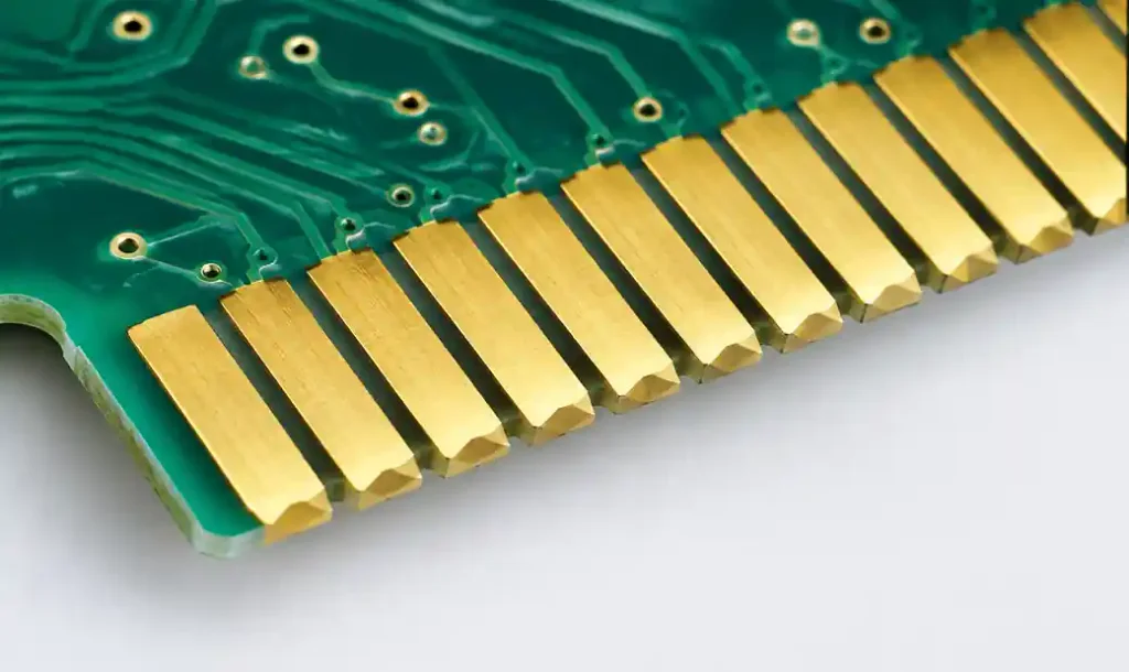
The term “hard gold” distinguishes electroplated gold (containing 5-10% cobalt or nickel hardener) from soft gold used in wire bonding. Hard gold achieves 130-200 Knoop hardness—three times harder than pure gold—enabling 500+ insertion cycles without wear-through. Standard thickness ranges from 30 to 50 microinches (0.76-1.27 μm), with 3-6 microinches nickel underplate providing diffusion barrier protection.
Hard Gold vs ENIG for Edge Connectors
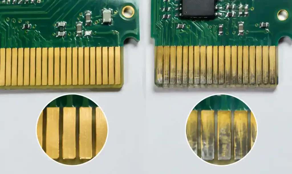
Selecting between electroplated hard gold and ENIG (Electroless Nickel Immersion Gold) determines connector durability and cost. ENIG deposits 2-4 microinches of soft gold over nickel through chemical immersion, creating excellent solder ability but limited wear resistance. After 20-50 insertion cycles, ENIG wears through to nickel, increasing contact resistance and causing intermittent failures.
| Surface Finish | Gold Thickness | Hardness (Knoop) | Insertion Cycles | Contact Resistance | Cost Premium |
|---|---|---|---|---|---|
| ENIG (Immersion Gold) | 2-4 μin (0.05-0.10 μm) | 60-90 | 20-50 | 15-30 mΩ after wear | Baseline |
| Electroplated Hard Gold | 30-50 μin (0.76-1.27 μm) | 130-200 | 500-1000 | <10 mΩ stable | +30-50% |
| Selective Hard Gold + ENIG | 30-50 μin fingers / 2-4 μin pads | 130-200 / 60-90 | 500-1000 fingers | <10 mΩ fingers | +20-35% |
Selective plating applies hard gold only to edge fingers while ENIG covers solderable pads, optimizing cost without sacrificing durability. A 4-layer PCB with 30 gold fingers and 200 component pads costs $12-18 per board with selective plating versus $25-35 for full hard gold at prototype quantities.
Gold Finger Plating Process and Standards
Manufacturing begins with copper pad definition during standard PCB fabrication. After solder mask application that exposes edge fingers, manufacturers apply nickel strike (50-100 microinches) through electroplating, creating adhesion layer and diffusion barrier. Hard gold electroplating follows, depositing cobalt-hardened gold to specified thickness per IPC-4552 and IPC-4553 standards.
Per IPC-6012 Class 2 requirements, gold thickness must meet 30 microinches minimum, while Class 3 (high-reliability) specifies 50 microinches. Nickel underplate prevents copper diffusion that causes contact resistance increase—copper migrating into gold creates intermetallic compounds with 50-100× higher resistivity than pure gold.
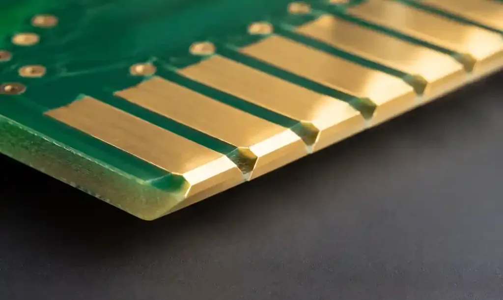
Edge beveling occurs after plating, typically at 30-45 degrees. The 45-degree bevel provides optimal insertion force distribution, requiring 20-40% less force than square edges while preventing PCB laminate delamination during insertion.
Design Rules for Reliable Gold Fingers
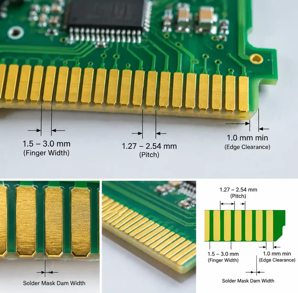
Finger geometry follows industry-standard dimensions to ensure connector compatibility. Standard finger width ranges from 1.5 to 3.0 mm, with 2.54 mm (0.100 inch) being most common for PCI/ISA applications. Finger spacing matches connector pitch—typically 1.27 mm, 2.0 mm, or 2.54 mm—with ±0.1 mm tolerance per IPC-2221.
Minimum copper clearance from board edge to first finger must exceed 1.0 mm. This clearance prevents copper exposure during beveling and accommodates manufacturing tolerances. Between adjacent fingers, maintain minimum 0.3 mm solder mask dam width to prevent solder bridging during assembly.
| Design Parameter | Minimum Value | Typical Value | Standard Reference |
|---|---|---|---|
| Finger Width | 1.5 mm (59 mil) | 2.0-2.54 mm (79-100 mil) | IPC-2221 |
| Finger Spacing (pitch) | 1.0 mm (39 mil) | 1.27-2.54 mm (50-100 mil) | IPC-2222 |
| Edge Clearance | 1.0 mm (39 mil) | 1.5-2.0 mm (59-79 mil) | IPC-2221 |
| Bevel Angle | 30° | 45° | Industry standard |
| Gold Thickness | 30 μin (0.76 μm) Class 2 | 50 μin (1.27 μm) Class 3 | IPC-6012 |
Finger length typically extends 3-10 mm from board edge, matching connector depth. Longer fingers increase mating reliability but consume board space—a trade-off between mechanical stability and PCB routing complexity.
Beveling and Edge Finishing Requirements
PCB edge beveling creates the angled lead-in surface essential for smooth connector insertion. Without beveling, square edges catch on connector pins, requiring 2-3× higher insertion force and risking PCB laminate damage. The standard 45-degree bevel reduces insertion force from 15-20N per finger to 6-10N while preventing edge delamination.
Manufacturing achieves beveling through CNC routing with chamfer mills after gold plating completes. Single-sided bevels work for most applications, but double-sided bevels (chamfered top and bottom) improve insertion from either direction—critical for reversible connectors like USB Type-C or certain M.2 modules.
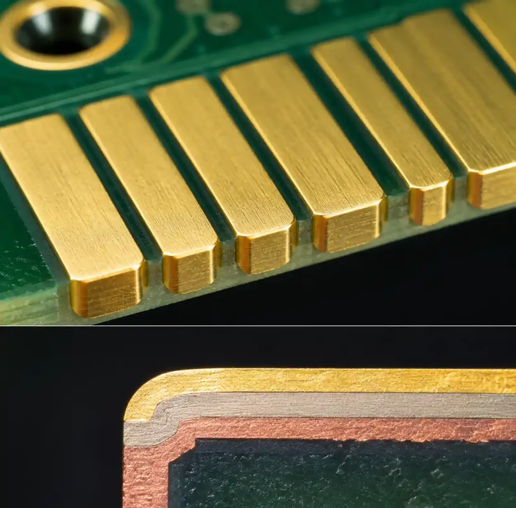
Edge finish quality directly affects connector life. Per IPC-6012, maximum edge roughness must stay below Ra 3.2 μm (125 microinches), measured after beveling. Rough edges create stress concentration points where gold cracks form, accelerating wear. Manufacturers verify edge quality through microscopy inspection at 50-100× magnification.
Signal Integrity Considerations for High-Speed Connectors
Gold fingers carrying high-speed signals above 1 GHz require impedance control to prevent reflections and signal degradation. Edge connector discontinuities create impedance spikes—reference plane gaps and finger geometry changes cause reflections that close eye diagrams in PCIe Gen3+ (8 GT/s) and DDR4/DDR5 applications.
Controlled impedance gold fingers maintain 50Ω ± 10% for single-ended or 100Ω ± 10% differential pairs through precise finger width and spacing. A 50Ω single-ended finger on standard FR4 (εr=4.3) requires approximately 0.9 mm trace width with 0.2 mm dielectric spacing to ground plane, assuming 1.6 mm board thickness.
Via transitions near gold fingers introduce additional inductance—each via adds 0.5-1.0 nH. At 5 GHz, 1 nH creates 31Ω impedance, causing 10-15% reflection. Minimize via stubs through back-drilling or blind vias in high-speed PCB design.
Applications: Memory Modules, Expansion Cards, and Industrial Systems
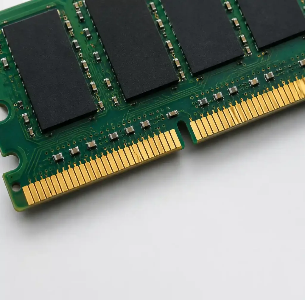
DDR5 memory modules: DIMM (Dual Inline Memory Module) designs use 288 gold fingers on 1.27 mm pitch, operating at 4800-6400 MT/s. Per JEDEC specifications, fingers must survive 50 insertion cycles minimum, with leading manufacturers specifying 100+ cycles for enterprise applications. Gold thickness typically reaches 50 microinches to ensure reliability across temperature cycling from -40°C to +85°C.
PCIe expansion cards: Graphics cards, NVMe SSDs, and network adapters employ PCIe edge connectors from ×1 (18 fingers) to ×16 (164 fingers). PCIe Gen5 at 32 GT/s requires strict impedance control with insertion loss below 15 dB at 16 GHz per PCI-SIG specifications. Hard gold with 30-50 microinches thickness maintains contact resistance below 5 milliohms throughout 100+ hotplug cycles.
Industrial control modules: Ruggedized systems for factory automation, railway, and military applications specify hard gold fingers with enhanced durability. MIL-PRF-55110 requires 1000+ insertion cycles with contact resistance remaining below 20 milliohms. These boards often use heavy copper PCB construction with 3-4 oz copper weight for power distribution alongside signal fingers.
Cost Factors and Manufacturing Lead Time
Gold finger cost scales primarily with gold thickness and plated area. Hard gold plating adds $0.40-0.80 per square inch at prototype quantities (5-10 boards), dropping to $0.15-0.30 per square inch above 500 units. A typical PCIe ×16 card with 164 fingers (approximately 4 square inches of gold) sees $1.60-3.20 premium for prototypes versus $0.60-1.20 in volume production.
Selective plating reduces costs 20-35% compared to full-board hard gold while maintaining edge connector durability. This approach applies hard gold only to fingers while ENIG covers solderable pads, optimizing finish for each application. Setup costs favor selective plating above 100 units—below this threshold, full ENIG with acceptance of limited connector cycles may prove more economical.
Lead time increases 2-3 days for hard gold plating versus standard ENIG. Quick turn PCB assembly providers deliver gold finger prototypes in 5-7 days, while production volumes ship in 10-15 days depending on complexity and layer count.
Common Gold Finger Defects and Prevention
Gold thickness variation: Uneven plating creates thin spots where wear-through occurs prematurely. Manufacturers verify thickness using X-ray fluorescence (XRF) at multiple points per finger. Per IPC-4553, thickness variation must stay within ±20% of specification. Proper plating rack design and current distribution prevent edge effects that cause 30-50% thickness reduction at finger corners.
Nickel diffusion: Insufficient nickel barrier allows copper to migrate into gold, forming copper-gold intermetallics with high resistance. This typically manifests after thermal cycling or high-temperature storage. Minimum 3 microinches nickel underplate per IPC-4552 prevents diffusion for 1000+ hours at 125°C.
Edge delamination: Inadequate edge finish or excessive bevel force causes laminate layers to separate. This occurs when router bit dull conditions create excessive heat or cutting force exceeds laminate bond strength. Specify fresh router bits every 500-1000 linear inches and verify edge quality through cross-sectional microscopy.
FAQ
What is the difference between hard gold and ENIG for gold fingers?
Hard gold (electroplated) provides 30-50 microinches thickness with 130-200 Knoop hardness, surviving 500-1000 insertion cycles. ENIG deposits only 2-4 microinches of soft gold, suitable for soldering but wearing through after 20-50 insertions. Choose hard gold for edge connectors and ENIG for solderable pads.
Why do gold fingers need beveling?
Beveling creates a 30-45 degree lead-in angle that guides the PCB into the connector smoothly, reducing insertion force by 50-70% and preventing laminate edge damage. Without beveling, square edges catch on connector pins, requiring excessive force that can crack solder joints or delaminate PCB edges.
Can I use ENIG instead of hard gold to reduce costs?
ENIG works for low-cycle applications (under 20 insertions) like one-time production test fixtures or rarely-removed modules. For field-serviceable components, memory modules, or expansion cards requiring 50+ cycles, hard gold is essential. Cost savings from ENIG (~30-50% less) disappear if connector failures require field returns.
What gold thickness do I need for 500 insertion cycles?
IPC-6012 Class 2 specifies 30 microinches minimum for general applications (300-500 cycles). Class 3 high-reliability applications require 50 microinches for 500-1000 cycles. Industrial and military specifications often mandate 50-75 microinches for extended durability beyond 1000 cycles per MIL-PRF-55110.
How does gold finger design affect signal integrity in high-speed applications?
Gold finger geometry creates impedance discontinuities that reflect signals above 1 GHz. Control finger width and spacing to maintain target impedance (50Ω single-ended, 100Ω differential). Minimize via stubs near connectors through back-drilling or blind vias. For PCIe Gen4+ or DDR5, insertion loss must stay below 15 dB per signal integrity standards.
Conclusion
Gold finger design requires balancing durability, signal integrity, and cost through proper plating specification and geometric design. Electroplated hard gold with 30-50 microinches thickness and 45-degree beveling provides 500-1000 insertion cycles for memory modules, expansion cards, and industrial control systems. Selective plating optimizes cost by applying hard gold only to edge fingers while ENIG covers solderable areas.
Design success depends on following IPC-6012 and IPC-4553 standards: maintain 1.0 mm minimum edge clearance, specify appropriate gold thickness for cycle requirements, and implement impedance control for high-speed signals above 1 GHz. Proper nickel underplate (3-6 microinches) prevents copper diffusion that degrades contact resistance over thermal cycling.
If you need gold finger PCBs for expansion cards, memory modules, or ruggedized industrial systems, Andwin Circuits offers advanced manufacturing with hard gold plating up to 50 microinches. Our selective plating process reduces costs 20-35% while maintaining connector durability exceeding 1000 cycles per IPC-6012 Class 3 standards. Fast delivery in 5-7 days for prototypes ensures your development schedule stays on track.
Contact us today for gold finger PCB manufacturing with precision plating control and competitive factory-direct pricing.