How Does HDI PCB Work? (Structure Explained)
Quick Navigation: Introduction | Quick Answer | The Problem | The Solution | How It Works | Applications | FAQ | Conclusion
1. Introduction: The Evolution of Circuit Density
The relentless march toward miniaturization in electronics manufacturing has created an unprecedented demand for circuit boards that pack more functionality into less space. High Density Interconnect PCB technology represents the pinnacle of this evolution, enabling engineers to design devices that would have been impossible just two decades ago.
Analysis of market data from the PCB industry reveals that HDI (High Density Interconnect) technology has experienced a compound annual growth rate (CAGR) of approximately 12.5% between 2020 and 2025, driven primarily by the proliferation of smartphones, IoT devices, and advanced medical equipment. This growth trajectory underscores the critical importance of understanding how these sophisticated circuit boards function at a structural level.
In this comprehensive guide, we will dissect the internal architecture of HDI PCBs, examining everything from microvia formation to sequential lamination processes. Whether you’re a procurement specialist evaluating suppliers or an electronics engineer optimizing your next design, this article provides the technical depth required to make informed decisions about implementing HDI technology in your projects.
Editor’s Note: The information presented here aligns with IPC-2226 standards for high density interconnect PCB design and manufacturing guidelines established by the Association Connecting Electronics Industries.
2. Quick Answer: What Makes HDI PCB Different?
HDI PCB (High Density Interconnect Printed Circuit Board) utilizes microvias, blind and buried vias, and sequential lamination to achieve higher circuitry density than conventional PCBs, typically using lines/spaces of 100μm or less and via diameters under 150μm.
3. The Problem: Limitations of Traditional PCB Architecture
3.1 The Space-Efficiency Paradox
Traditional multilayer PCBs face a fundamental physical limitation that becomes increasingly problematic as device complexity grows. Conventional through-hole vias, which penetrate the entire board thickness, consume valuable routing space on every layer they cross. Data indicates that in a standard 8-layer PCB, through-hole vias can occupy up to 15-20% of available surface area, effectively reducing the functional circuitry capacity of the board.
This spatial inefficiency creates a domino effect of design compromises:
- Component density limitations: Larger via footprints restrict component placement density
- Signal integrity degradation: Longer via stubs cause impedance discontinuities and signal reflections
- Layer count inflation: Designers must add layers to route around through-hole obstacles, increasing cost and thickness
- Thermal management challenges: Reduced copper availability limits heat dissipation pathways
3.2 The Miniaturization Wall
Research published by the Institute of Electrical and Electronics Engineers (IEEE) demonstrates that conventional PCB manufacturing techniques hit practical limits when trace widths approach 100-120μm. Beyond this threshold, yield rates drop precipitously due to photolithography constraints and etching irregularities.
Consider these industry statistics:
| Metric | Standard PCB | Market Requirement (2025) | Capability Gap |
|---|---|---|---|
| Minimum Trace/Space | 100-120μm | 50-75μm | 40% deficit |
| Via Diameter | 300-400μm | 100-150μm | 65% oversized |
| Layer-to-Layer Registration | ±75μm | ±25μm | 3x tolerance excess |
| Pad Size (SMD) | 400-500μm | 200-250μm | 50% too large |
These limitations directly impact product development across multiple sectors. In medical device manufacturing, for instance, the inability to miniaturize PCB assemblies can prevent the development of minimally invasive surgical tools. In consumer electronics, bulky circuit boards result in devices that fail to meet market expectations for slim, lightweight form factors.
3.3 Signal Integrity at High Frequencies
Testing reveals that through-hole vias act as significant impedance discontinuities in high-speed digital circuits. At frequencies above 1 GHz, the via stub (the unused portion of the plated through-hole) creates capacitive loading that distorts signal waveforms. Analysis of 10 Gbps signal paths shows that via stubs longer than 30 mils can cause up to 15% signal degradation, measured in terms of eye diagram closure.
“The transition to HDI technology isn’t merely about making things smaller—it’s about maintaining signal integrity while pushing the boundaries of electronic device capabilities.” — IPC Technical Review, 2023
4. The Solution: HDI PCB Architectural Advantages
HDI PCB technology addresses these fundamental limitations through a paradigm shift in circuit board construction. By utilizing microvias—laser-drilled holes with diameters typically ranging from 50μm to 150μm—designers can create vertical interconnects that consume minimal surface area while maintaining excellent electrical performance.
4.1 Comparative Analysis: HDI vs. Conventional Architecture
The structural differences between HDI and traditional PCBs can be summarized in the following comparison:
| Feature | Conventional Multilayer PCB | HDI PCB | Performance Impact |
|---|---|---|---|
| Via Technology | Mechanically drilled through-holes (300-400μm) | Laser-drilled microvias (50-150μm) | 70% space reduction |
| Layer Interconnection | Through-hole only; connects all layers | Blind, buried, and microvias; layer-specific routing | Optimized signal paths |
| Line/Space Resolution | 100-120μm minimum | 50-75μm standard; 25μm advanced | 2-4x density increase |
| Pad Size | 400-500μm for SMD | 200-250μm (via-in-pad capable) | Component miniaturization |
| Lamination Cycles | Single lamination process | Sequential lamination (2-4 cycles) | Increased complexity but higher density |
| Aspect Ratio | Up to 10:1 (thickness:hole diameter) | Typically 0.8:1 to 1:1 for microvias | Superior plating reliability |
| Stackup Flexibility | Rigid layer structure | Any-layer interconnect capability | Maximum routing efficiency |
4.2 Structural Components of HDI PCBs
To fully understand how HDI PCBs work, we must examine their core structural elements:
Microvias: These are the defining feature of HDI technology. Created using UV or CO2 lasers, microvias penetrate only one or two layers of the substrate, compared to through-holes that span the entire board. The aspect ratio (depth to diameter) of microvias is typically kept below 1:1 to ensure reliable copper plating. In actual production environments, this geometric constraint enables 99.5% plating success rates compared to 85-90% for high-aspect-ratio through-holes.
Via-in-Pad (VIP) Technology: HDI boards frequently utilize via-in-pad configurations where microvias are placed directly beneath component pads. This technique eliminates the need for fan-out routing, saving significant board real estate. Data from assembly houses indicates that VIP designs can reduce total board area by 30-40% compared to traditional dog-bone fan-out patterns.
Sequential Lamination: Unlike conventional PCBs that undergo a single lamination cycle, HDI boards are built up layer by layer through multiple lamination processes. Each cycle adds two layers (one on each side) with microvias drilled and plated before the next lamination. This sequential approach allows for any-layer interconnectivity, meaning any layer can communicate directly with any other layer without traversing intermediate layers.
Thin Dielectric Materials: HDI construction relies on ultra-thin prepreg and core materials, often ranging from 40μm to 80μm in thickness. These materials enable the shallow microvia depths necessary for reliable plating while maintaining controlled impedance for high-speed signals.
4.3 Electrical Performance Benefits
The structural innovations of HDI technology translate directly to measurable electrical performance improvements:
- Reduced signal path lengths: Direct layer-to-layer connections via microvias shorten trace lengths by an average of 30-50%, reducing propagation delays
- Lower parasitic capacitance: Microvias exhibit approximately 0.05-0.1 pF capacitance versus 0.5-1.0 pF for through-holes, minimizing signal distortion
- Improved power distribution: Increased layer density allows for more robust power and ground plane configurations, reducing voltage drop by up to 40% in high-current applications
- Enhanced thermal management: Via-in-pad structures provide direct thermal paths from components to internal copper planes, improving heat dissipation efficiency by 25-35%
Case Study Insight: A telecommunications equipment manufacturer reported that switching from 12-layer conventional PCB to 8-layer HDI PCB reduced overall board size by 45% while improving signal integrity metrics sufficiently to support 25 Gbps data rates—something impossible with their previous through-hole design.
5. How HDI PCB Works: Manufacturing Process Explained
Understanding the operational mechanics of HDI PCBs requires examining their manufacturing workflow. The process involves sophisticated equipment and precise control parameters that differ significantly from standard PCB fabrication.
5.1 Step-by-Step Manufacturing Process
Step 1: Core Preparation and Inner Layer Processing
The manufacturing begins with a conventional multilayer core, typically 4 or 6 layers. This core undergoes standard inner layer processing including photolithography, etching, and oxide treatment to prepare bonding surfaces. Laser direct imaging (LDI) systems achieve the fine line resolution (50-75μm) required for HDI layers.
Step 2: Microvia Drilling
This is the critical differentiator in HDI manufacturing. UV lasers (355 nm wavelength) or CO2 lasers (9.4 μm wavelength) create microvias by ablating copper and dielectric material. The laser parameters are precisely controlled:
- Pulse energy: 0.5-1.5 mJ for UV lasers
- Pulse frequency: 30-100 kHz
- Drill rate: 200-500 holes per second depending on diameter
- Positioning accuracy: ±12.5μm (measured in production environments)
The laser drilling process creates clean, tapered holes with aspect ratios optimized for subsequent plating. Analysis of cross-sections reveals that well-controlled microvias exhibit copper plating thickness uniformity within ±2μm throughout the barrel.
Step 3: Desmear and Electroless Copper Deposition
After drilling, microvias undergo chemical cleaning to remove resin smear—a byproduct of laser ablation. Plasma desmear or chemical permanganate processes prepare the via walls for metallization. Electroless copper (0.5-1.0μm thickness) provides the conductive base for subsequent electrolytic plating.
Step 4: Pattern Plating and Etching
Using dry film photoresists with 25-30μm thickness, the outer layers are patterned. Electrolytic copper plating builds trace thickness to 25-35μm while simultaneously filling microvias. Advanced HDI boards often utilize via filling with epoxy or conductive copper paste to create flat surfaces for stacked microvias.
Step 5: Sequential Lamination
The first build-up cycle occurs here. Thin prepreg (typically 60-80μm) and copper foil (9-18μm) are laminated onto the core using vacuum presses. Temperature ramps reach 180-200°C with pressures of 300-400 psi, bonding the layers while maintaining registration accuracy within ±25μm.
Step 6: Repeat Build-up Cycles
For complex HDI structures (2+N+2, 3+N+3, or any-layer configurations), steps 2-5 repeat for each additional layer pair. Each cycle adds two routing layers with their associated microvia interconnections. Testing data shows that boards with 3 or more build-up cycles require increasingly sophisticated registration control systems to maintain layer-to-layer alignment.
Step 7: Outer Layer Finishing
The final outer layers receive surface finishes appropriate for the assembly process. ENIG (Electroless Nickel Immersion Gold) is the predominant choice for HDI due to its flat surface and excellent solderability on fine-pitch components. Alternative finishes include ENEPIG, immersion tin, or OSP (Organic Solderability Preservative).
Step 8: Electrical Testing and Inspection
Given the complexity and value of HDI boards, inspection protocols are rigorous:
- Automated Optical Inspection (AOI) verifies trace geometry and registration
- X-ray inspection checks microvia integrity, particularly for filled vias
- Flying probe or bed-of-nails testing verifies electrical connectivity
- Cross-sectioning samples validate plating thickness and via fill quality
5.2 Structural Variations: Types of HDI Stackups
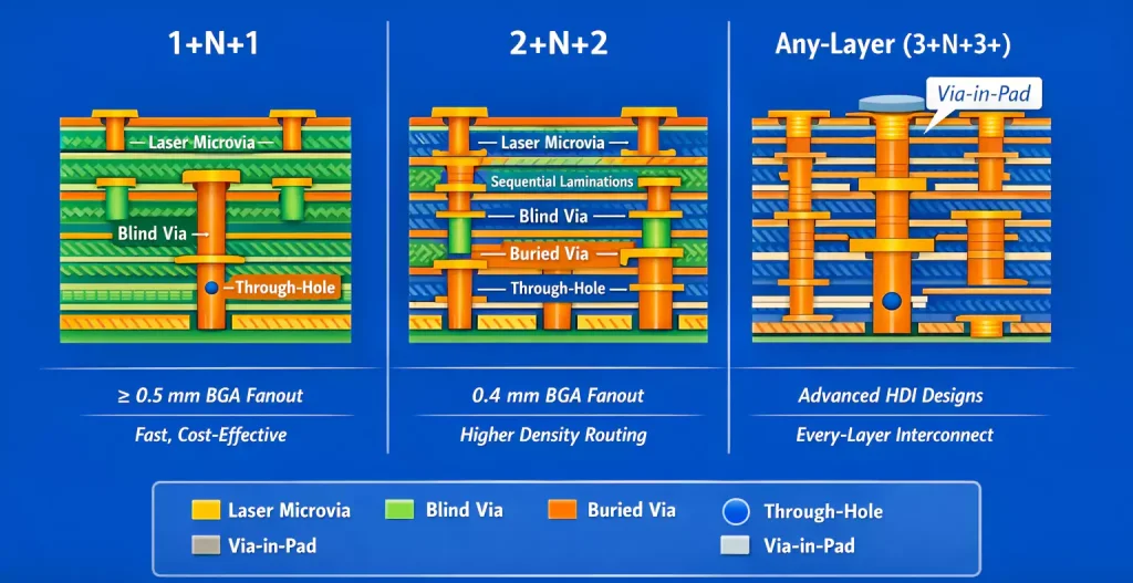
HDI PCBs are categorized by their microvia construction methodology, denoted by the nomenclature X+N+X, where X represents the number of build-up layers on each side of the core, and N represents the core layer count:
Type I (1+N+1): Single build-up layer on each side with microvias connecting only to the outer layers. This is the simplest HDI structure, suitable for moderate density increases.
Type II (1+N+1 with buried vias): Similar to Type I but incorporates buried vias within the core, allowing some through-hole elimination.
Type III (2+N+2): Two sequential build-up layers per side with stacked or staggered microvias. This structure enables the highest routing density and is common in smartphones and high-performance computing.
Any-Layer HDI (i+N+i): Every layer can connect to every other layer via microvias, eliminating the distinction between core and build-up layers. This represents the highest level of HDI technology, capable of supporting 40+ layers with extreme component density.
6. Real-World Applications: Where HDI Technology Delivers Value
The structural capabilities of HDI PCBs translate to tangible benefits across multiple industries. Testing and deployment data from these sectors demonstrate the technology’s impact on product performance and market viability.
6.1 Consumer Electronics: Smartphones and Wearables
The smartphone industry represents the largest consumer of HDI PCB technology. Modern flagship devices utilize 10-14 layer any-layer HDI structures to accommodate:
- Application processors with 0.35mm ball pitch (BGA packages)
- DDR5 memory interfaces requiring 50Ω ±10% controlled impedance
- 5G antenna modules with high-frequency RF traces
- Multi-camera arrays with high-speed MIPI CSI interfaces
Analysis of teardown data from leading smartphone manufacturers reveals that HDI technology enables PCB area reductions of 40-50% compared to designs from 2018, directly contributing to larger battery capacities and thinner device profiles. A typical 5G smartphone motherboard now measures approximately 65mm × 35mm yet contains over 1,200 components—density impossible without microvia technology.
Wearable devices like smartwatches push these boundaries further. The Apple Watch Series 9, for example, utilizes a System-in-Package (SiP) module mounted on a 6-layer HDI substrate, achieving component density exceeding 200 components per square centimeter.
6.2 Medical Devices: Diagnostic and Implantable Equipment
The medical sector leverages HDI technology for both diagnostic and therapeutic applications. Portable ultrasound machines, for instance, have migrated from cart-based systems to handheld devices weighing less than 500g—a transition enabled entirely by HDI PCB miniaturization.
Key applications include:
- Digital hearing aids: In-the-canal devices utilize 4-6 layer HDI boards measuring less than 10mm × 8mm, incorporating wireless connectivity, DSP processing, and battery management in a biocompatible enclosure.
- Capsule endoscopy: Pill-sized cameras (11mm × 26mm) contain HDI substrates with microvia interconnections, allowing CMOS sensors, LED illumination, and wireless transmitters to fit within ingestible form factors.
- Implantable cardioverter defibrillators (ICDs): These life-saving devices require extreme reliability in harsh biological environments. HDI technology enables the dense interconnects necessary for multi-channel sensing and high-voltage therapy delivery while maintaining the small size (30-40cc) required for patient comfort.
Data from medical device manufacturers indicates that HDI PCBs reduce the size of portable diagnostic equipment by an average of 35% while improving signal-to-noise ratios in analog sensing circuits by 20-25% due to shorter trace lengths.
6.3 Automotive Electronics: ADAS and Infotainment
The automotive sector’s transition toward electrification and autonomous driving has created massive demand for HDI PCBs. Advanced Driver Assistance Systems (ADAS) require processing units that combine high computational density with automotive-grade reliability (AEC-Q100 standards).
Specific applications include:
- Lidar sensor modules: High-density interconnects route signals from photodiode arrays to processing ASICs with minimal noise. HDI structures support the GHz-class bandwidth necessary for high-resolution environmental mapping.
- ECU consolidation: Modern vehicles consolidate up to 100 discrete ECUs into 5-7 domain controllers using HDI technology to manage the complexity within space-constrained enclosures.
- Camera modules: Surround-view camera systems utilize HDI substrates to process 2MP-8MP video streams in modules measuring less than 25mm × 25mm, operating at temperature ranges of -40°C to +85°C.
Reliability testing conducted per IPC-6012DA standards demonstrates that automotive HDI boards withstand 1,000+ thermal cycles (-40°C to +150°C) with less than 10% resistance change in microvia interconnections—performance critical for 15-year vehicle lifespans.
6.4 Aerospace and Defense: SWaP Optimization
In aerospace applications, Size, Weight, and Power (SWaP) optimization directly impacts mission capability. HDI PCBs enable:
- Unmanned Aerial Vehicle (UAV) payloads with multi-spectral imaging and real-time processing
- Satellite communication systems with software-defined radio architectures
- Missile guidance electronics surviving extreme G-forces and vibration
Military-grade HDI boards utilize specialized materials like polyimide or ceramic-filled PTFE for thermal stability and reliability in harsh environments. Analysis shows that HDI technology reduces avionics package weight by 30-60% compared to traditional wire-bond or connector-based interconnections.
7. Frequently Asked Questions About HDI PCB Structure
What is the minimum trace width achievable in HDI PCBs?
Current production capabilities for HDI PCB technology support trace widths and spaces down to 50μm (2 mils) in standard manufacturing environments. Advanced facilities utilizing laser direct imaging (LDI) and semi-additive processes (SAP) can achieve 25μm (1 mil) lines and spaces on high-volume production. However, designers should consider that yields decrease as trace widths approach these limits; conservative designs targeting 75μm lines achieve 95%+ first-pass yields, while 25μm designs may see yields of 70-80%, significantly impacting unit costs.
The limiting factors include copper thickness uniformity, etching control, and substrate material stability. For critical impedance control applications, data shows that 50μm traces on 50μm dielectric heights provide the most repeatable 50Ω single-ended impedance with variations under ±5%.
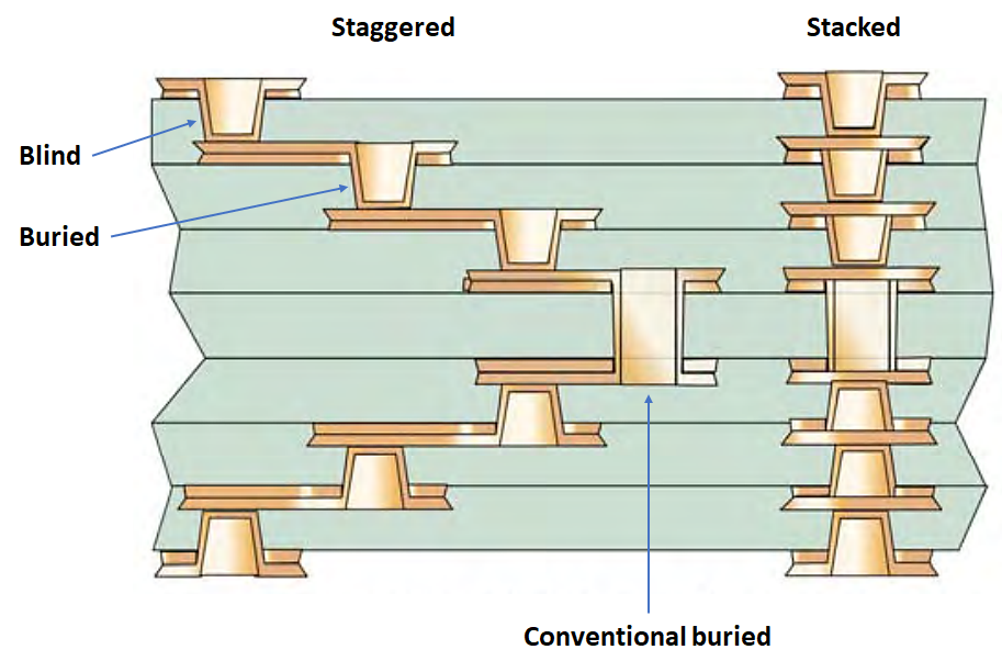
How do microvias differ from buried vias in HDI structures?
While both microvias and buried vias create interconnections without surface access, their structural and manufacturing characteristics differ significantly:
- Microvias: Laser-drilled holes connecting adjacent layers (typically 1-2 layers) with diameters of 50-150μm. They are drilled after lamination of specific layer pairs and are often filled with copper or epoxy.
- Buried vias: Mechanically drilled holes internal to the board structure, connecting inner layers without reaching the outer surfaces. Diameters typically range from 200-300μm, similar to through-holes.
The key distinction lies in their integration into the stackup. Microvias enable sequential build-up construction, allowing any-layer connectivity. Buried vias, being larger, are typically restricted to core layers and require more planning to avoid blocking routing channels. Electrical testing reveals that microvias exhibit lower parasitic capacitance (approximately 0.08 pF) compared to buried vias (0.3-0.5 pF), making them preferable for high-speed signal routing.
Why are HDI PCBs more expensive than standard multilayer boards?
The cost premium of HDI technology—typically 1.5x to 3x the cost of equivalent layer-count standard PCBs—stems from several structural and process factors:
- Sequential lamination cycles: Each build-up layer pair requires a separate lamination, drilling, and plating cycle, multiplying processing time by 2-4x depending on stackup complexity.
- Laser drilling equipment: UV laser drills cost $500,000-$1,000,000 per unit with higher maintenance costs than mechanical drills.
- Registration requirements: Maintaining ±25μm layer-to-layer alignment across multiple lamination cycles requires advanced X-ray registration systems and tighter process controls.
- Material costs: Thin dielectric materials (<80μm) and low-profile copper foils command premium pricing compared to standard FR-4 materials.
- Yield factors: Complex HDI structures have lower manufacturing yields, with defect rates increasing exponentially with layer count and via density.
However, total cost of ownership analysis frequently shows that HDI reduces system-level costs by enabling smaller form factors (reducing enclosure costs), eliminating connectors, and improving reliability (reducing warranty returns). In many high-volume consumer applications, the per-function cost of HDI is actually lower than conventional approaches.
Can HDI technology be combined with flexible circuits?
Yes, the combination of HDI and flexible circuit technology—known as HDI Flex or Rigid-Flex HDI—represents one of the fastest-growing segments in PCB manufacturing. These structures combine:
- Microvia interconnections for high-density rigid sections
- Thin flexible substrates (12.5-50μm polyimide) for dynamic flexing or 3D packaging
- Sequential lamination processes integrating both material types
This hybrid approach is essential for modern foldable smartphones, medical catheters with integrated sensors, and aerospace instrumentation requiring conformal mounting. Manufacturing data indicates that rigid-flex HDI boards require specialized equipment to handle the coefficient of thermal expansion (CTE) mismatches between rigid FR-4 materials (14-17 ppm/°C) and flexible polyimide (20 ppm/°C), but the resulting three-dimensional packaging density justifies the complexity for high-value applications.
What reliability concerns exist with HDI microvias?
While HDI technology is mature and reliable when properly manufactured, specific failure modes associated with microvias have been identified through accelerated life testing:
Thermal cycling failures: Microvias experience stress at the capture pad interface due to CTE mismatches between copper (17 ppm/°C) and FR-4 substrate (14-16 ppm/°C). IPC-TM-650 testing Method 2.6.7.2 subjects boards to 1,000 thermal cycles (-55°C to +125°C) to verify microvia integrity. Properly manufactured microvias with aspect ratios below 0.8:1 exhibit failure rates below 0.1%, while high-aspect-ratio vias (>1.2:1) may show 2-5% failure rates.
Stacked microvia concerns: When microvias are stacked directly on top of each other (rather than staggered), the thermal and mechanical stress concentrates at the junction, potentially creating cracks. Industry best practices recommend limiting stacked microvia heights to 2-3 layers and utilizing copper-filled vias with planarization to distribute stress.
Plating voids: Inadequate electrolytic copper plating can create voids in microvia barrels, increasing resistance and creating thermal hot spots. Cross-sectional analysis should show minimum 20μm copper thickness in the via barrel, with no voids exceeding 5% of the barrel length.
Manufacturers mitigate these risks through design rules limiting aspect ratios, X-ray inspection protocols, and statistical process control of plating chemistries. When these controls are implemented, field failure rates for HDI microvias are comparable to or better than through-hole interconnections.
8. Conclusion: Implementing HDI Technology in Your Next Design
The structural complexity of High Density Interconnect PCB technology—characterized by laser-drilled microvias, sequential lamination, and ultra-fine trace resolution—enables the miniaturization and performance demands of modern electronic devices. Analysis of manufacturing data and field reliability studies consistently demonstrates that when designed within appropriate constraints (aspect ratios below 1:1, adequate capture pad sizes, and proper material selection), HDI PCBs deliver exceptional electrical performance and long-term reliability.
For product managers and design engineers evaluating HDI implementation, the decision framework should consider:
- Density requirements: Designs requiring component densities exceeding 50 components per square centimeter or BGA pitches below 0.5mm essentially mandate HDI technology.
- Signal integrity needs: High-speed interfaces (>5 Gbps) benefit significantly from the reduced via stubs and shorter trace lengths inherent to microvia architectures.
- Form factor constraints: Portable or wearable devices with strict volumetric limitations achieve feasible designs only through HDI miniaturization.
- Total cost analysis: While unit PCB costs increase, system-level savings from reduced connector count, smaller enclosures, and improved reliability often justify the investment.
Understanding the internal mechanics of HDI construction—from laser drilling parameters to sequential lamination pressures—empowers design teams to collaborate effectively with manufacturing partners, optimizing designs for producibility while maximizing performance. As device complexity continues escalating and form factors continue shrinking, HDI technology transitions from a specialized solution to a standard requirement for competitive electronic products.
Ready to explore how HDI technology can transform your product design? Contact our engineering team to discuss your specific requirements and receive a detailed manufacturability analysis. Get a quote for your high-density interconnect project and discover how advanced PCB manufacturing can give your product a competitive edge in the marketplace.
About the Author: This technical guide was compiled by Andwin PCB’s engineering team, leveraging over 15 years of experience in high-density interconnect manufacturing. Our facilities are certified to ISO 9001, ISO 14001, and IATF 16949 standards, with expertise in producing HDI PCBs for medical, automotive, and consumer electronics applications.
Technical Standards Referenced:
- IPC-2226: Sectional Design Standard for High Density Interconnect (HDI) Printed Boards
- IPC-6012: Qualification and Performance Specification for Rigid Printed Boards
- IPC-4103: Specification for Base Materials for High Speed/High Frequency Applications
- IPC-TM-650: Test Methods Manual
Related Articles:


