
Industrial PCB Design for Vibration and Shock Resistance
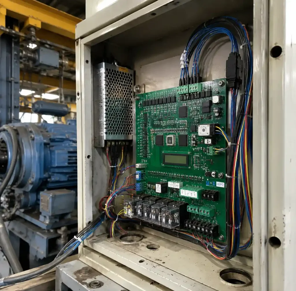
Industrial control systems operate in environments where vibration and mechanical shock are constant threats. Studies show that up to 25% of industrial equipment failures trace back to PCB-related mechanical stress issues. Factory floors, transportation equipment, and outdoor installations subject circuit boards to forces that can crack solder joints and dislodge components within months.
If you want to design industrial PCBs that survive harsh mechanical environments, you need to understand component stress analysis, strain relief techniques, mounting strategies, and testing per IEC 60068 standards. This guide provides actionable design rules from industrial automation and transportation applications.
What Is Vibration and Shock Resistance in Industrial PCB Design?
Vibration resistance refers to a PCB’s ability to withstand cyclic mechanical forces without functional degradation. According to IEC 60068-2-6, vibration testing subjects boards to sinusoidal motion from 10 Hz to 500 Hz, simulating motor vibration and machinery operation. Shock resistance, defined in IEC 60068-2-27, measures survival under sudden mechanical impact with peak accelerations from 15g to 100g.
These stresses create fatigue in solder joints, crack copper traces at stress points, and can dislodge surface-mount devices. Industrial PCBs must withstand 15-25 years of continuous operation, making mechanical design as critical as electrical performance. You should specify vibration-resistant design when equipment operates near motors or moving machinery, or when boards mount in vehicles or outdoor enclosures.
Component Mechanical Stress and Fatigue Resistance
Solder joints fail under vibration through cumulative fatigue damage. When a board flexes, components with high mass experience inertial forces proportional to weight multiplied by acceleration. A 50-gram transformer at 3g vibration sees 150 grams of force cyclically applied thousands of times daily.
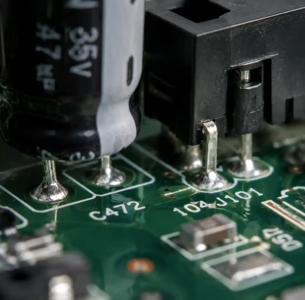
Component standoff height affects stress concentration. Ball grid arrays with 0.5mm standoffs distribute stress better than SOT-23 devices with 0.2mm joint height. Through-hole components generally outperform surface-mount devices because mechanical leads provide strain relief and larger solder fillets absorb flexural energy before fracturing.
Large electrolytic capacitors above 1000µF, power transformers, and heavy connectors represent the highest failure risk. Their mass creates significant inertial loads during board flex. Fine-pitch BGAs concentrate stress in tiny solder joints that crack after 10^5 to 10^6 load cycles. You should implement additional support for any component exceeding 10 grams.
| Component Type | Vulnerability | Mitigation | Mass Threshold |
|---|---|---|---|
| Electrolytic capacitors >1000µF | High | Epoxy staking, horizontal mount | >5g |
| Power transformers | Very High | Bracket mounting, potting | >15g |
| Heavy connectors | Very High | Strain relief, edge reinforcement | >8g |
| BGAs <0.5mm pitch | High | Underfill, via-in-pad | N/A |
Strain Relief for Connectors and Heavy Components
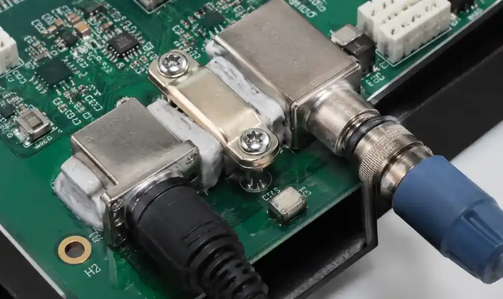
Epoxy staking around connector mounting pins provides the most effective strain relief. Apply rigid epoxy (Shore D 80-90) bonding the connector body to PCB surface and encapsulating solder joints. This transfers mechanical loads from individual joints to the board substrate. For connectors with repeated mating cycles, use flexible epoxy (Shore A 60-70) that accommodates insertion forces.
Metal brackets bolted through the PCB distribute connector loads across multiple mounting points. Industrial manufacturers use L-brackets attaching to both connector shell and board with M3 hardware. These must allow 0.5mm movement using compliance washers to prevent rigid coupling during thermal cycling.
Via-in-pad technology underneath large component pads improves both thermal relief and mechanical strength. Copper-filled vias create solid thermal and mechanical paths through the board, reducing stress concentration. Specify filled and capped vias for components above 5 grams in vibration applications.
Mount high-force connectors within 5mm of board edges with supporting material extending to the edge. Keep critical circuits at least 15mm away from connector mounting areas where board flex concentrates. Orient rectangular connectors so their long axis aligns parallel to dominant vibration direction, minimizing moment arm and reducing solder joint bending stress.
Board Support and Mounting Strategies
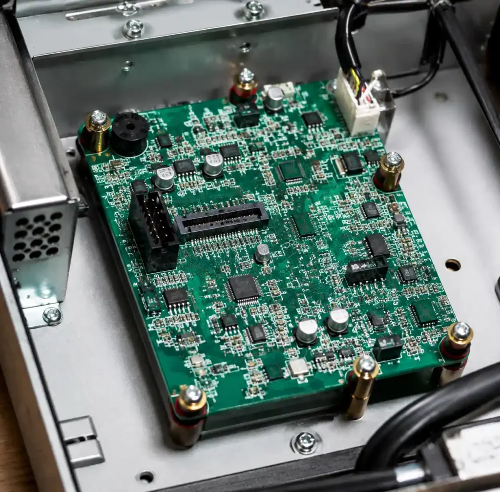
Industrial PCBs require minimum four mounting points for boards larger than 100 cm², with additional points every 150 cm² of area. IEC 60068 assumes mounting point spacing not exceeding 150mm for standard boards and 100mm for high-density designs. Mounting holes should be 3.2mm diameter for M3 hardware, positioned 5mm from edges.
Vibration-damping grommets or standoffs reduce transmitted shock from enclosure to PCB. Silicone or neoprene grommets with 40-60 Shore A hardness provide optimal isolation for frequencies above 50 Hz. Metal standoffs with spring washers offer superior long-term reliability in high-temperature environments where elastomers degrade.
Increasing PCB thickness from 1.6mm to 2.0mm significantly improves stiffness and reduces flexural displacement. Bending stiffness scales with the cube of thickness, so a 2.0mm board is 95% stiffer than 1.6mm. Metal stiffening ribs or aluminum backing plates bonded to PCB backside dramatically increase bending resistance while improving thermal management.
| Board Size (mm) | Mounting Points | Max Spacing (mm) | Thickness (mm) |
|---|---|---|---|
| 100 × 100 or smaller | 4 corners | 100 | 1.6 |
| 150 × 150 | 4 corners | 150 | 1.6-2.0 |
| 200 × 150 | 6 perimeter | 100 | 2.0 |
| 250 × 200+ | 8+ grid | 100 | 2.0-2.4 |
Potting and Encapsulation for Maximum Protection
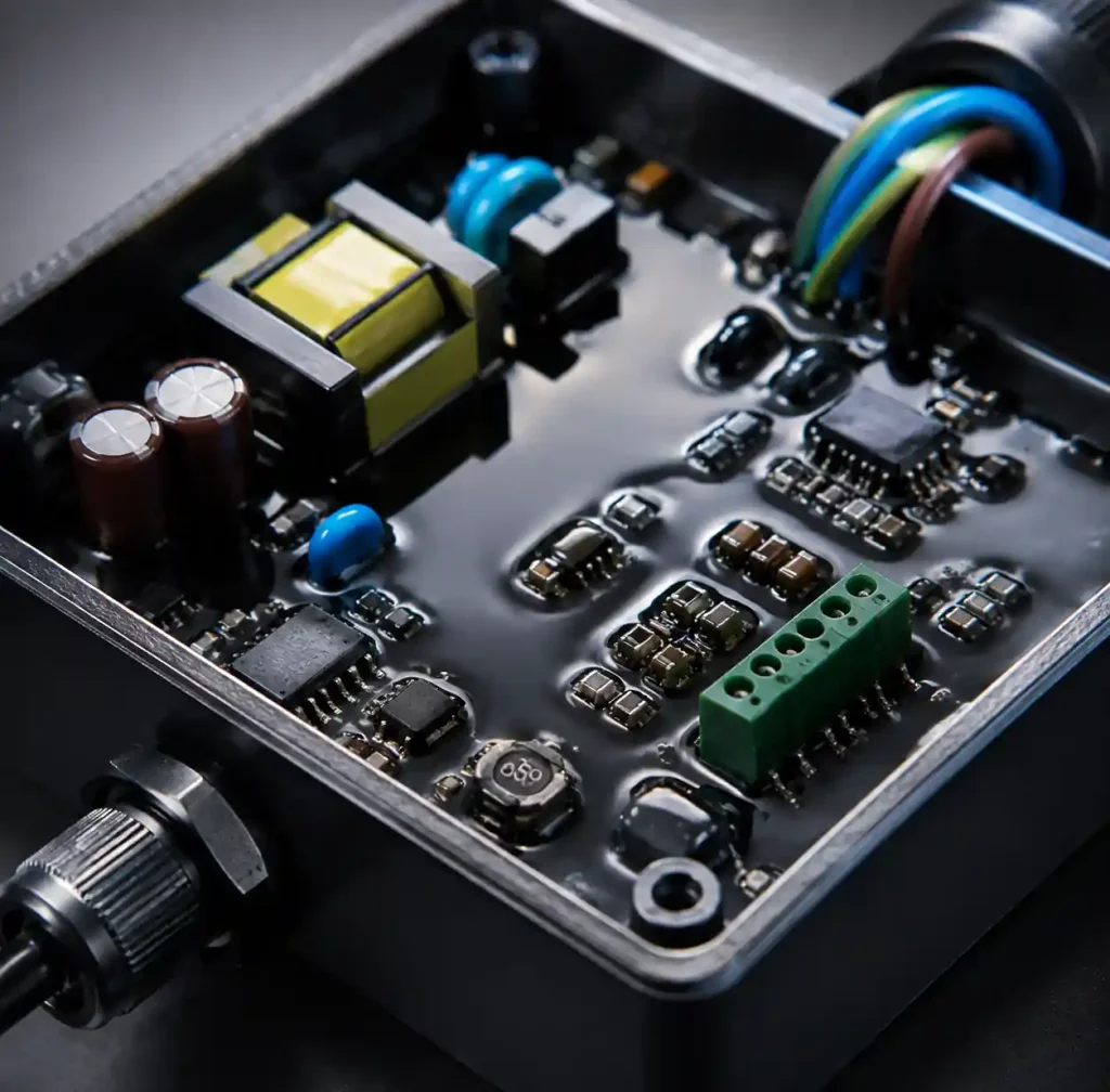
Epoxy potting compounds offer maximum mechanical strength with Shore D hardness 75-85. Two-part epoxies cure to form rigid structures that lock components in place and distribute stress across the assembly. Thermal conductivity ranges from 0.6 to 3 W/mK with thermally enhanced formulations. Epoxy provides excellent moisture barrier but makes rework impossible.
Polyurethane compounds balance protection with rework capability. With Shore A hardness 60-90, polyurethanes absorb vibration energy while allowing component flexing. You can remove polyurethane by cutting or chemical dissolution. Silicone encapsulants provide maximum flexibility (Shore A 20-60) and operate across the widest temperature range (-60°C to +200°C).
Selective potting encapsulates only high-risk components while leaving the rest accessible. Apply compound around connector joints, large capacitors, and power components. This maintains 70-80% of full potting’s benefit while preserving test point access. Full board encapsulation maximizes protection by creating a monolithic structure eliminating all internal movement.
Material Selection for Fatigue Resistance
High-Tg FR-4 with glass transition temperatures from 170°C to 180°C provides mechanical stability for industrial environments. Standard FR-4 (130-140°C Tg) softens at elevated temperatures, reducing flexural modulus. Higher Tg maintains stiffness across the full -40°C to +85°C industrial range, reducing component stress by 20-30%.
Metal core PCBs using aluminum substrates offer superior vibration resistance through increased stiffness. A 1.5mm aluminum core board provides 5-10 times the stiffness of equivalent FR-4. The metal core also acts as thermal spreader and EMI shield.
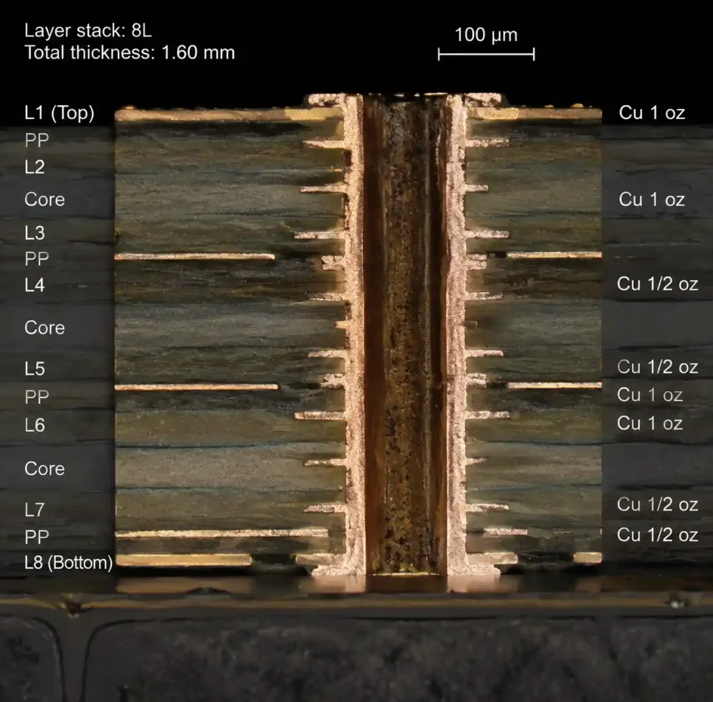
Specify 2oz (70µm) or heavier copper to increase trace mechanical strength and reduce fatigue cracking. Thicker copper traces resist crack propagation from stress points. Filled vias prevent barrel cracking by eliminating hollow cylinder structure. Copper-filled or resin-filled vias create solid mechanical connections through the board stackup, extending fatigue life by 3-5× in high-vibration applications.
Testing Per IEC 60068-2-6 and IEC 60068-2-27
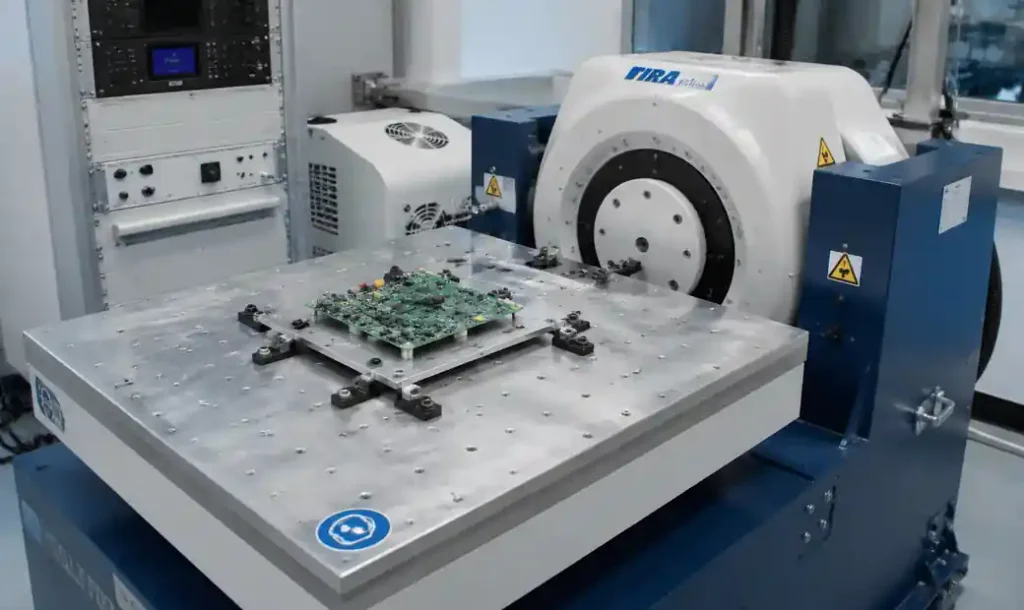
IEC 60068-2-6 defines sinusoidal vibration testing with frequency sweeps from 10 Hz to 500 Hz across three orthogonal axes. Industrial equipment typically requires 1g to 2g acceleration, while transportation applications demand 3g to 5g. Test duration ranges from 10 cycles per axis for screening to 100+ cycles for qualification.
The standard specifies logarithmic frequency sweep rates of one octave per minute. Monitor electrical functionality during vibration using go/no-go indicators because intermittent failures during vibration often precede permanent damage. Natural frequencies of board and components appear as peaks in response spectrum.
Mechanical shock testing subjects assemblies to half-sine pulses with peak values from 15g to 100g and durations from 6ms to 30ms. Transportation specifications typically require 30g half-sine shocks with 11ms duration applied three times per axis in both directions—18 total shocks. Testing must occur with the board mounted in operational configuration using actual mounting hardware.
Pass criteria include electrical functionality checks after each shock and visual inspection for physical damage. Cracks in solder joints, delamination, and component displacement constitute failures even if immediate function remains intact.
Design Checklist for Vibration-Resistant PCBs
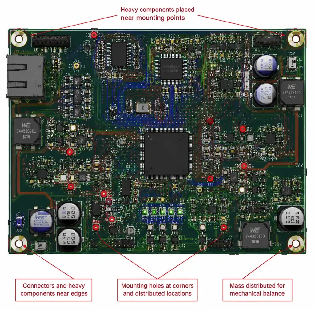
Locate heavy components near mounting points where board displacement is minimal. Distribute mass evenly to avoid creating high-inertia regions. Orient components so their longest dimension aligns with the board’s highest stiffness direction.
Route traces with gradual curves rather than sharp 90-degree angles near high-stress zones. Avoid routing critical traces directly beneath heavy components where board flex concentrates. Solder joint profiles must achieve full intermetallic formation without voids. Automated optical inspection should flag solder joints with insufficient fillet height on vibration-critical components.
FAQs
Which IEC standards apply to industrial PCB vibration testing?
IEC 60068-2-6 covers sinusoidal vibration testing from 10-500 Hz. IEC 60068-2-27 defines mechanical shock testing with peak accelerations from 15g to 100g. IEC 60068-2-64 specifies broadband random vibration testing simulating real-world exposure.
How thick should industrial PCBs be for vibration resistance?
Minimum 1.6mm thickness works for small boards under 100 cm² with proper mounting. Boards 150-250 cm² should use 2.0mm thickness. Larger control boards benefit from 2.4mm construction. Stiffness increases with the cube of thickness.
Which components need strain relief in vibration environments?
All components above 5 grams require epoxy staking or mechanical reinforcement. Connectors regardless of weight need strain relief. BGAs with pitch below 0.5mm should use underfill. Through-hole components above 20 grams benefit from bracket mounting.
When should you use potting instead of conformal coating?
Conformal coating provides moisture protection with 25-125µm thickness but offers minimal mechanical reinforcement. Potting with 3-10mm compound thickness locks components in place and dramatically improves vibration resistance. Use potting when mechanical stress is the primary concern.
How often should vibration testing occur during development?
Perform initial testing on first prototype builds to identify design weaknesses. Repeat testing after mechanical or component placement changes. Production qualification requires testing per IEC 60068 at expected severity levels plus 50% margin.
Conclusion
Industrial PCB designs surviving high-vibration environments require attention to component stress, strain relief, board mounting, material selection, and encapsulation. IEC 60068 testing provides objective verification before field deployment. Key principles include appropriate board thickness, strain relief for heavy components, high-Tg materials with heavier copper, and selective or full potting based on stress levels.
Andwin Circuits manufactures industrial control PCBs with vibration-resistant designs up to 2.4mm thickness using high-Tg FR-4 and metal core substrates. Our assembly services include epoxy staking, selective potting, and conformal coating for harsh-environment protection. Testing capabilities per IEC 60068-2-6 and IEC 60068-2-27 verify design robustness. For industrial control applications requiring extended operating life in mechanical stress environments, our design-for-reliability approach ensures your equipment meets field performance requirements.
Contact us today for industrial PCB manufacturing and assembly services with factory-direct pricing.