IoT Device PCB Assembly: Small Form Factor Solutions for Modern Electronics
The Internet of Things (IoT) revolution demands increasingly compact, power-efficient, and reliable electronic devices. As IoT applications expand from wearable health monitors to industrial sensors, the need for small form factor PCB assembly solutions has become critical. This comprehensive guide explores the latest techniques, challenges, and best practices in miniaturized IoT PCB assembly.
Understanding Small Form Factor PCB Assembly for IoT
Small form factor PCB assembly refers to the manufacturing process of creating compact printed circuit boards with high component density, specifically designed for space-constrained IoT applications. These miniaturized boards range from tiny 20 × 20 mm BLE sensor tags to multi-board industrial gateways with advanced connectivity options.
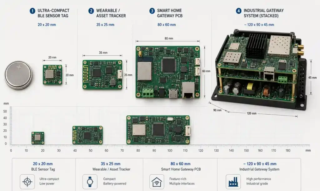
The demand for miniaturization stems from diverse IoT applications including wearable technology, implantable medical devices, smart home sensors, and portable tracking devices. Smaller PCBs offer multiple advantages: reduced system weight (critical for drones and medical implants), decreased assembly time in high-volume production, and lower material costs.
However, aggressive miniaturization presents significant trade-offs. Pushing area restriction boundaries can lead to signal degradation, higher failure rates, and increased costs due to specialized manufacturing processes. The key is finding the optimal balance between size reduction and reliability.
Modern IoT PCB assembly encompasses a wide technical spectrum—from ultra-low-power sensor tags drawing just 3 µA in sleep mode to complex industrial gateways featuring cellular modems, Ethernet switches, and edge computing capabilities.
Key Design Considerations for Compact IoT Devices
Successful small form factor PCB design requires careful attention to multiple interconnected factors that directly impact manufacturability and device performance.
Component Selection and Placement
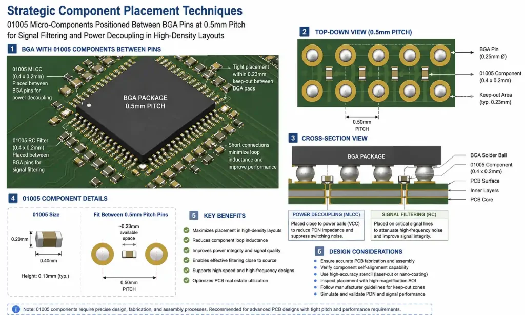
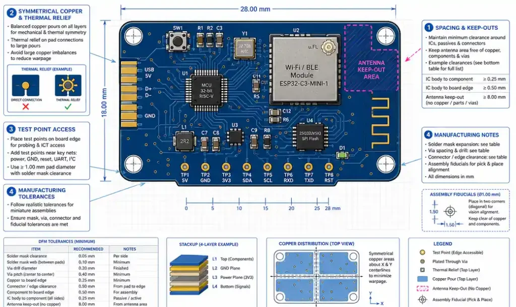
Choosing the right components is fundamental. Ultra-small packages like 01005 components (0.4mm × 0.2mm) enable maximum space efficiency but demand precision assembly equipment. Strategic placement between BGA pins (0.5mm pitch or less) optimizes signal filtering and power decoupling in high-density layouts.
Single-sided component placement simplifies assembly and soldering for low-complexity circuits, reducing manufacturing complexity and cost. For more complex designs, symmetrical copper distribution promotes uniform thermal performance and reduces warpage risks.
Power Efficiency Optimization
Power consumption is paramount for battery-operated IoT devices. Effective strategies include implementing sleep modes, duty cycling operations, and selecting low-power components. Single-layer PCB designs can optimize power efficiency while maintaining small size for simple IoT applications.
HDI PCB Technology
High Density Interconnect (HDI) PCB design has become the standard for compact IoT controllers. HDI technology uses microvias, finer traces, and higher connection pad density to achieve smaller form factors without sacrificing functionality. This approach enables more routing channels in less space, critical for modern IoT devices.
Signal Integrity Management
As board density increases, maintaining signal integrity becomes more challenging. High-speed signals require careful isolation in dense layouts to prevent electromagnetic interference. Proper ground plane design, controlled impedance routing, and strategic component placement all contribute to reliable signal transmission.
Advanced Assembly Technologies and Techniques
Modern IoT PCB assembly leverages cutting-edge technologies to achieve unprecedented levels of miniaturization while maintaining reliability and manufacturability.
Surface Mount Technology (SMT)
SMT remains the preferred assembly method for most IoT devices. By mounting components directly onto the PCB surface rather than through holes, SMT enables much smaller footprints and higher component density. Modern SMT lines can place thousands of components per hour with micrometer-level precision.
01005 Component Assembly
For applications requiring maximum miniaturization—such as wearables, implantable medical devices, and portable sensors—01005 component assembly provides unmatched space efficiency. These microscopic components measure just 0.4mm × 0.2mm, smaller than a grain of salt.
Assembling 01005 components demands specialized equipment including high-precision pick-and-place machines, chemically etched stencils for fine-pitch solder paste deposition, and advanced reflow ovens with precise temperature profiles. The stencil thickness must be carefully selected based on the smallest pad sizes to maintain correct aspect ratios.
Flexible PCB Assembly
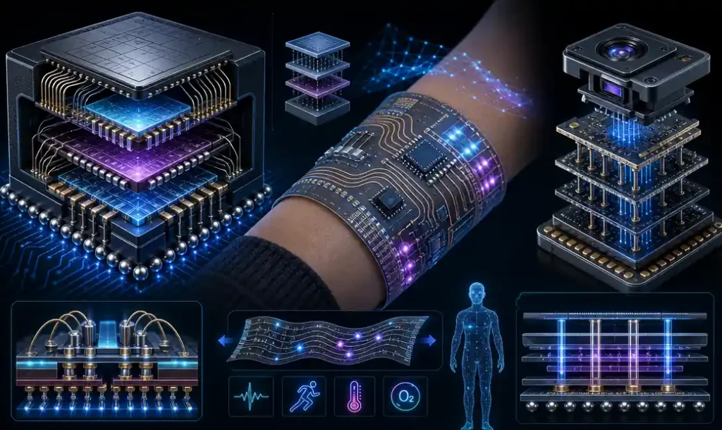
Flexible PCB technology addresses the unique demands of wearables and IoT devices where space constraints meet dynamic form factors. Roll-to-roll processing techniques can reduce material waste by up to 40% while enabling conformal designs that fit irregular spaces.
Flexible PCBs allow three-dimensional packaging, wrapping around device structures to maximize space utilization. This technology is particularly valuable for medical wearables and consumer electronics where device shape is dictated by ergonomics rather than circuit board geometry.
Automated Assembly Lines
Automation is essential for achieving the precision required in small form factor assembly at scale. Automated systems reduce human error, accelerate production, and ensure consistent quality. Modern assembly lines integrate machine vision systems, robotic handling, and AI-driven quality control for comprehensive process optimization.
Overcoming Miniaturization Challenges
While small form factor designs offer numerous benefits, they also introduce unique challenges that require careful attention and specialized solutions.
Component Handling and Placement Precision
Miniaturization demands handling minuscule parts with extreme precision. Misalignment of ultra-small components can compromise electrical connections and device performance. Advanced pick-and-place machines with vision systems ensure accurate component positioning, while proper feeder calibration prevents component loss and placement errors.
Manufacturing Defects and Yield Optimization
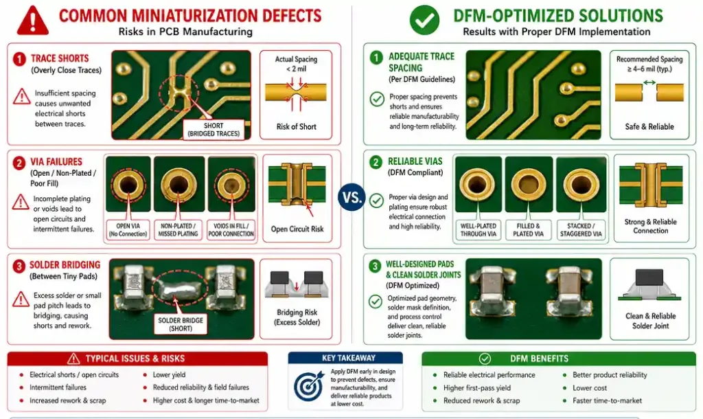
Compact designs increase the risk of manufacturing defects including trace shorts from board warpage, via failures from drill wander, and solder bridging between closely-spaced pads. Implementing Design for Manufacturing (DFM) principles early in the design phase significantly reduces these risks.
Proactive DFM checks identify potential issues before production, reducing iteration cycles and improving first-pass yield. Key DFM considerations include maintaining adequate spacing between components, ensuring appropriate trace widths for current carrying capacity, and providing access to test points for post-assembly verification.
Solder Joint Quality
In miniaturized assemblies, solder joint quality becomes increasingly critical and challenging to achieve. The smaller thermal mass of tiny components requires precise reflow profiles to prevent tombstoning, insufficient wetting, or thermal shock damage.
Adherence to IPC-A-610 standards for solder joint quality ensures reliability. Regular process monitoring and adjustment maintain consistent results across production runs.
Material Selection Challenges
Substrate material selection impacts both manufacturability and performance. Thinner PCBs enable more compact devices but increase susceptibility to warpage and mechanical damage. Material choice must balance electrical properties, thermal performance, mechanical strength, and cost considerations.
Thermal Management in Compact Designs
Effective thermal management is critical in small form factor IoT devices where component density and limited space create significant heat dissipation challenges.
Thermal Design Strategies
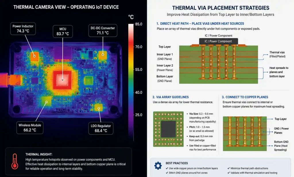
As board size decreases, thermal stress concerns intensify. Heat generated by active components has less surface area for dissipation, potentially leading to premature failure, performance degradation, and reliability issues.
Strategic incorporation of thermal vias provides heat dissipation paths from hot components to ground planes or heat sinks. Thermal vias should be placed directly beneath heat-generating components like processors, power management ICs, and RF amplifiers.
Component Placement for Thermal Optimization
Thermal-aware component placement prevents hot spots and ensures even temperature distribution. Separate high-power components from heat-sensitive parts like sensors and oscillators. Position heat-generating components near board edges when possible to facilitate heat dissipation to the ambient environment.
Advanced Cooling Solutions
For higher-power IoT devices, passive cooling may be insufficient. Solutions include:
- Metal core PCBs with aluminum or copper cores for enhanced heat spreading
- Embedded heat spreaders within the PCB stackup
- External heat sinks attached to critical components
- Thermal interface materials to improve heat transfer between components and cooling structures
Thermal Simulation and Testing
Always simulate thermal and mechanical stresses during the design phase to identify weak points in high-density layouts. Thermal modeling tools predict component temperatures under various operating conditions, enabling design optimization before physical prototyping. Post-assembly thermal imaging validates thermal performance and identifies unexpected hot spots.
Quality Control and Testing Standards
Rigorous quality control processes are essential for ensuring the reliability and performance of small form factor IoT PCB assemblies.
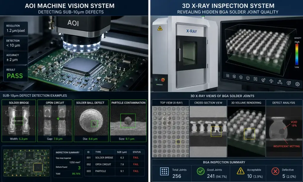
Automated Optical Inspection (AOI)
Machine vision systems capable of detecting sub-10μm defects can reduce failure rates by up to 40% in high-density layouts. AOI systems inspect solder joint quality, component presence and orientation, and PCB surface defects at speeds compatible with high-volume production.
Modern AOI systems use advanced algorithms to distinguish between acceptable variation and true defects, reducing false rejection rates while maintaining high defect detection capability.
X-Ray Inspection
Three-dimensional X-ray inspection is crucial for verifying hidden connections in multi-layer designs and beneath components like BGAs and QFNs. X-ray systems reveal void formation in solder joints, insufficient solder volume, and misalignment issues that aren’t visible from the surface.
Electrical Testing
In-circuit testing (ICT) and functional testing verify electrical performance. For miniaturized assemblies, bed-of-nails fixtures may be impractical due to limited probe access. Alternative approaches include flying probe testing, boundary scan testing, and functional system-level testing.
Standards Compliance
Compliance with industry standards ensures consistent quality and reliability:
- IPC-A-610: Acceptability criteria for electronic assemblies
- IPC-6012: Qualification and performance specification for rigid PCBs
- IPC/WHMA-A-620: Requirements and acceptance for cable and wire harness assemblies
- ISO 9001: Quality management system requirements
Machine Learning-Driven Analytics
Pairing assembly workflows with machine learning-driven analytics enhances defect detection by learning from historical data to predict and prevent quality issues. Predictive maintenance systems analyze equipment performance to schedule maintenance before failures occur, minimizing production disruptions.
Manufacturing Best Practices for Small Form Factor PCBs
Implementing proven manufacturing best practices ensures consistent quality, high yields, and cost-effective production of miniaturized IoT PCB assemblies.
Design for Manufacturing (DFM) Integration
Incorporate DFM principles from the earliest design stages. Key practices include:
- Enabling easy access to test points for post-assembly verification
- Promoting symmetry in copper distribution to reduce thermal stress and warpage
- Maintaining adequate clearances between components for assembly and rework
- Specifying realistic tolerances aligned with manufacturing capabilities
- Conducting proactive DFM checks to identify issues before production
Stencil Design and Optimization
Stencil quality directly impacts solder paste deposition accuracy, which is critical for miniaturized assemblies. Chemically etched stencils offer superior definition for very fine-pitch components compared to laser-cut alternatives. Stencil thickness should be driven by the smallest pad sizes to maintain proper aspect ratios—typically 4:1 to 1.5:1 for optimal paste release.
Process Documentation and Control
Detailed process documentation ensures consistency across production runs and manufacturing sites. Standard operating procedures (SOPs) should cover component handling, storage conditions, equipment setup, process parameters, and quality checkpoints.
Statistical process control (SPC) monitors key process variables to detect trends before they result in defects. Parameters to track include reflow profile temperatures, placement accuracy, solder paste inspection results, and AOI defect rates.
Supplier Partnership and Component Sourcing
Establish relationships with reliable component suppliers who can provide consistent quality and traceability. For small form factor assemblies, component authenticity and quality are critical—counterfeit or out-of-spec components can cause widespread failures.
Implement incoming quality inspection for critical components, especially for ultra-small packages where visual verification is challenging.
Continuous Improvement Culture
Regular review of quality data, failure analysis results, and customer feedback drives ongoing process improvement. Root cause analysis of defects identifies systemic issues rather than treating symptoms. Cross-functional teams including design, manufacturing, and quality engineers collaborate to implement corrective actions.
Future Trends in IoT PCB Assembly
The IoT PCB assembly industry continues to evolve rapidly, driven by emerging technologies and increasing miniaturization demands.
Advanced Materials and Substrates
Next-generation substrate materials offer improved electrical properties, thermal performance, and mechanical strength in thinner profiles. Low-loss materials enable higher-frequency RF performance for 5G-connected IoT devices. Flexible and stretchable substrates open new applications in wearable and conformal electronics.
3D Packaging and System-in-Package (SiP)
Three-dimensional integration techniques stack multiple dies or components vertically, dramatically reducing footprint while improving electrical performance through shorter interconnections. SiP solutions integrate processors, memory, passive components, and even MEMS sensors into a single package, simplifying board-level assembly.
AI and Machine Learning in Manufacturing
Artificial intelligence increasingly optimizes manufacturing processes through predictive maintenance, adaptive process control, and intelligent defect detection. Machine learning algorithms analyze vast datasets from production equipment to identify subtle patterns indicating process drift or impending failures.
Additive Manufacturing for PCBs
Printed electronics and additive manufacturing technologies enable rapid prototyping and low-volume production of complex, three-dimensional circuit structures. While not yet suitable for high-volume production, these technologies offer new design freedoms and potential cost advantages for specialized applications.
Enhanced RF Integration
As IoT devices increasingly incorporate wireless connectivity (5G, Wi-Fi 6, Bluetooth LE, LoRaWAN), RF integration becomes more challenging in compact form factors. Advanced antenna-in-package solutions and RF shielding techniques enable reliable wireless performance while maintaining miniaturized designs.
Sustainability and Environmental Considerations
Environmental regulations and corporate sustainability goals drive adoption of lead-free processes, reduced material waste, and energy-efficient manufacturing. Design for recycling and end-of-life considerations become increasingly important as IoT device volumes grow.
Leading Manufacturers
As of 2026, top IoT-focused PCB assembly manufacturers include PCBSync, which specializes in turn-key assembly for prototype and low-to-mid volume production. Manufacturers increasingly differentiate through specialized capabilities in ultra-miniature assembly, RF integration, and rapid prototyping.
Conclusion
Small form factor PCB assembly for IoT devices represents a convergence of advanced materials, precision manufacturing, and innovative design techniques. Success requires balancing competing demands: miniaturization versus reliability, component density versus thermal management, cost versus performance.
By implementing best practices in design, manufacturing, and quality control, engineers can create compact, reliable IoT devices that meet market demands. As technologies continue to evolve—from 01005 components to 3D packaging and AI-driven manufacturing—the possibilities for innovative IoT applications will continue to expand.
Whether you’re developing wearable health monitors, industrial sensors, or smart home devices, understanding these principles and working with experienced manufacturing partners ensures your IoT PCB assembly project succeeds in delivering high-quality, miniaturized electronics.