
Manufacturability Issues in PCB Routing Layers
Introduction
Printed Circuit Boards (PCBs) are the backbone of modern electronics, providing the necessary electrical connections between components. The routing layers of a PCB play a critical role in ensuring signal integrity, power distribution, and overall functionality. However, poor routing practices can lead to significant manufacturability issues, affecting yield, reliability, and cost. This article explores the key manufacturability challenges in PCB routing layers, including trace width/spacing, via placement, impedance control, thermal management, and design for manufacturability (DFM) considerations.
1. Trace Width and Spacing Issues
1.1 Minimum Trace Width Violations
PCB manufacturers have specific capabilities regarding the smallest trace width they can reliably produce. If traces are too narrow:
- Etching Problems: Over-etching can cause open circuits, while under-etching may lead to short circuits.
- Current Carrying Capacity: Thin traces may not handle high currents, leading to overheating and failure.
- Impedance Mismatch: High-speed signals require controlled impedance, which depends on trace width. Incorrect widths can degrade signal quality.
1.2 Insufficient Trace Spacing
Inadequate spacing between traces can cause:
- Short Circuits: Due to manufacturing tolerances, closely spaced traces may bridge during etching or soldering.
- Crosstalk: High-speed signals can interfere with adjacent traces if spacing is insufficient.
- Voltage Breakdown: High-voltage designs require larger spacing to prevent arcing.
Solution: Follow the manufacturer’s Design Rule Check (DRC) guidelines for minimum trace width and spacing.
2. Via-Related Manufacturing Challenges
2.1 Via Size and Placement
- Drilling Limitations: Small vias (< 0.2mm) may be difficult to drill, increasing cost and failure rates.
- Via-in-Pad Issues: Placing vias directly under components can cause solder wicking, leading to poor solder joints.
- Annular Ring Problems: Insufficient copper around via holes can result in broken connections after drilling.
2.2 Via Stitching and Thermal Relief
- Poor Via Stitching: Inadequate via stitching in ground/power planes increases impedance and EMI.
- Thermal Relief Absence: Vias connected to large copper pours without thermal relief can cause soldering difficulties due to heat dissipation.
Solution: Use appropriate via sizes, avoid via-in-pad unless necessary, and implement thermal relief connections.
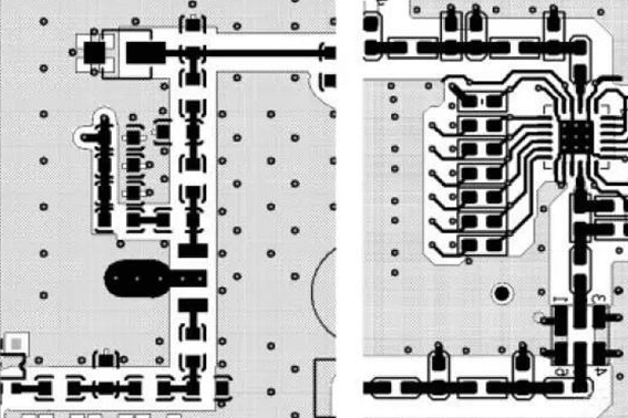
3. Impedance Control and Signal Integrity
3.1 Mismatched Trace Impedance
High-speed signals (e.g., USB, HDMI, DDR) require controlled impedance traces. Issues include:
- Incorrect Dielectric Thickness: Impedance depends on PCB stack-up; wrong material or thickness alters impedance.
- Uneven Trace Geometry: Variations in trace width or copper thickness affect impedance.
3.2 Return Path Discontinuities
- Split Planes: High-speed signals crossing plane splits create EMI and signal integrity problems.
- Inadequate Grounding: Poor return paths increase noise and crosstalk.
Solution: Use impedance calculators, maintain consistent trace geometry, and ensure continuous return paths.
4. Thermal Management and Copper Balancing
4.1 Uneven Copper Distribution
- Warpage: Uneven copper layers can cause PCB warping during reflow soldering.
- Etching Variability: Dense copper areas etch differently than sparse regions, leading to over/under-etching.
4.2 Thermal Relief in Power Planes
- Poor Heat Dissipation: Large copper areas without thermal relief make soldering difficult.
- Thermal Stress: Uneven heating can damage components or delaminate layers.
Solution: Balance copper distribution, use thermal relief pads, and follow symmetric layer stack-ups.
5. Design for Manufacturability (DFM) Considerations
5.1 Acid Traps and Sharp Angles
- Acid Traps: Acute angles in traces can trap etching chemicals, leading to over-etching.
- 90-Degree Corners: These can cause impedance discontinuities and EMI in high-speed designs.
Solution: Use 45-degree angles or curved traces instead of sharp corners.
5.2 Silkscreen and Solder Mask Issues
- Misaligned Silkscreen: Poor labeling can lead to assembly errors.
- Solder Mask Bridging: Inadequate solder mask between pads can cause shorts.
Solution: Ensure proper solder mask expansion and silkscreen clearance.
5.3 Panelization and Fiducial Marks
- Poor Panelization: Incorrect breakaway tabs or spacing can damage PCBs during depaneling.
- Missing Fiducials: Lack of alignment marks leads to pick-and-place errors.
Solution: Include fiducials and follow panelization best practices.

6. Material and Layer Stack-Up Challenges
6.1 Incorrect Material Selection
- High-Frequency Losses: Standard FR-4 may not be suitable for RF/microwave applications.
- Thermal Expansion Mismatch: Different materials expand at varying rates, risking delamination.
6.2 Improper Layer Stack-Up
- Cross-Talk Between Layers: Adjacent signal layers should be orthogonal to reduce interference.
- Power/Ground Plane Separation: Insufficient decoupling leads to noise.
Solution: Choose appropriate materials and optimize layer stack-up for signal integrity.
Conclusion
PCB routing layer manufacturability depends on careful design practices that account for trace geometry, via placement, impedance control, thermal management, and DFM principles. Ignoring these factors can lead to fabrication defects, assembly failures, and reduced product reliability. By adhering to industry standards and collaborating with manufacturers, designers can ensure high-yield, cost-effective PCB production.