
Medical PCB for Implantable Devices: Hermetic Sealing and Biocompatibility
Implantable medical devices represent a critical segment of healthcare technology, with over 30 million devices implanted globally each year. These life-sustaining electronics depend on PCBs that must function flawlessly inside the human body for 10 to 15 years. Understanding hermetic sealing and biocompatibility is essential for engineers designing next-generation implantable devices.
What Are Medical PCBs for Implantable Devices?
Medical PCBs for implantable devices are specialized circuit boards designed to operate continuously inside the human body while maintaining absolute reliability and biocompatibility. These boards feature hermetically sealed packages protecting sensitive electronics from bodily fluids—saline and slightly acidic environments that rapidly corrode conventional PCB materials.
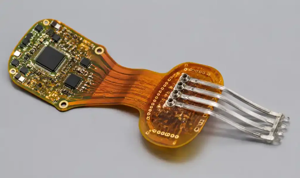
Implantable circuits must meet ISO 10993 biocompatibility standards and ISO 13485 quality requirements. The PCB integrates with hermetic feedthroughs—glass-to-metal or ceramic-to-metal seals—allowing electrical connections while maintaining moisture barriers.
You can use rigid-flex PCB technology for implantable devices because it reduces assembly complexity and improves reliability. Studies show rigid-flex assemblies achieve failure rates 8× lower than connector-based systems with lifespans exceeding 15 years.
Biocompatibility Requirements: ISO 10993 Standards
ISO 10993 is the internationally recognized standard for biological evaluation of medical devices. The FDA issued guidance on ISO 10993-1 in September 2023, establishing evaluation protocols within a risk management framework.

For implantable PCBs, biocompatibility testing evaluates cytotoxicity (cell viability), sensitization (allergic response), irritation (tissue reaction), systemic toxicity (organ effects), genotoxicity (DNA damage), implantation response (long-term tissue compatibility), and carcinogenicity for permanent implants.
Material Selection for Body Fluid Exposure
Polymer encapsulation faces bio-fluid penetration challenges, a primary failure mode for implantable electronics. You should select materials providing diffusion barriers while maintaining biocompatibility.
Biocompatible substrate materials include polyimide (Kapton) with excellent chemical resistance for neural interfaces, PEEK with high mechanical strength for orthopedic implants, parylene coating offering nanometer-level conformal barriers, and medical-grade epoxies certified USP Class VI for bodily fluid contact.
Research shows standard PCB materials can be viable when properly encapsulated, offering reliability advantages and cost reduction compared to custom substrates.
Corrosion Resistance for Body Fluid Exposure
Bodily fluids create a hostile environment with 0.9% saline and pH 7.35-7.45. Standard finishes like HASL or OSP corrode rapidly when exposed. You should specify corrosion-resistant finishes:
| Surface Finish | Corrosion Resistance | Biocompatibility | Typical Use |
|---|---|---|---|
| ENIG (Gold) | Excellent | Validated | Pacemakers, neurostimulators |
| Hard Gold Plating | Superior | Excellent | Feedthrough contacts |
| Platinum/Iridium | Outstanding | Proven | Electrode arrays |
| Titanium Nitride | Excellent | Validated | Neural electrodes |
Hermetic Packaging Technologies
Glass-to-Metal Seals
Glass-to-metal seals provide vacuum-tight barriers while allowing electrical connections through hermetic packages. These compression bonds between metal pins and glass insulators withstand decades of bodily fluid exposure.
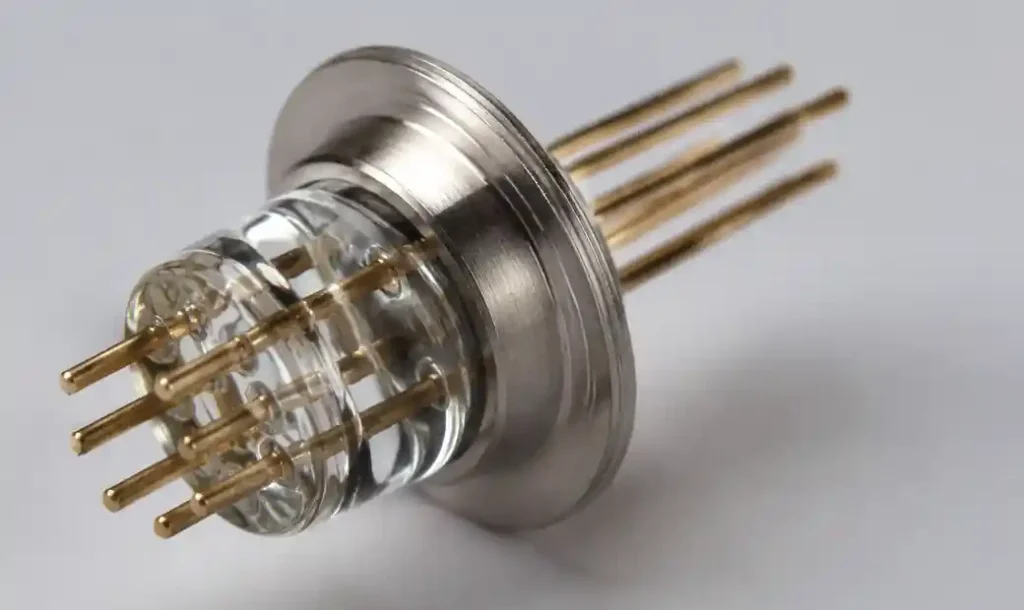
Manufacturing uses specialized sealing glasses with thermal expansion coefficients matched to biocompatible metals like titanium or stainless steel. Glass composition contains silicon dioxide, boron oxide, and alkali oxides softening at 400-500°C during sealing without degrading metal components.
Ceramic Hermetic Packages
Ceramic packages offer superior hermeticity for implantable electronics. High Temperature Co-fired Ceramic (HTCC) technology enables multilayer structures with integrated feedthroughs and heat dissipation in compact millimeter-scale packages.
Ceramic packages provide helium leak rates below 1×10⁻⁸ atm·cc/sec per MIL-STD-883, biocompatible alumina (Al₂O₃) or zirconia (ZrO₂) materials, thermal conductivity 20-30 W/mK for heat dissipation, and laser welding compatibility for titanium lids.
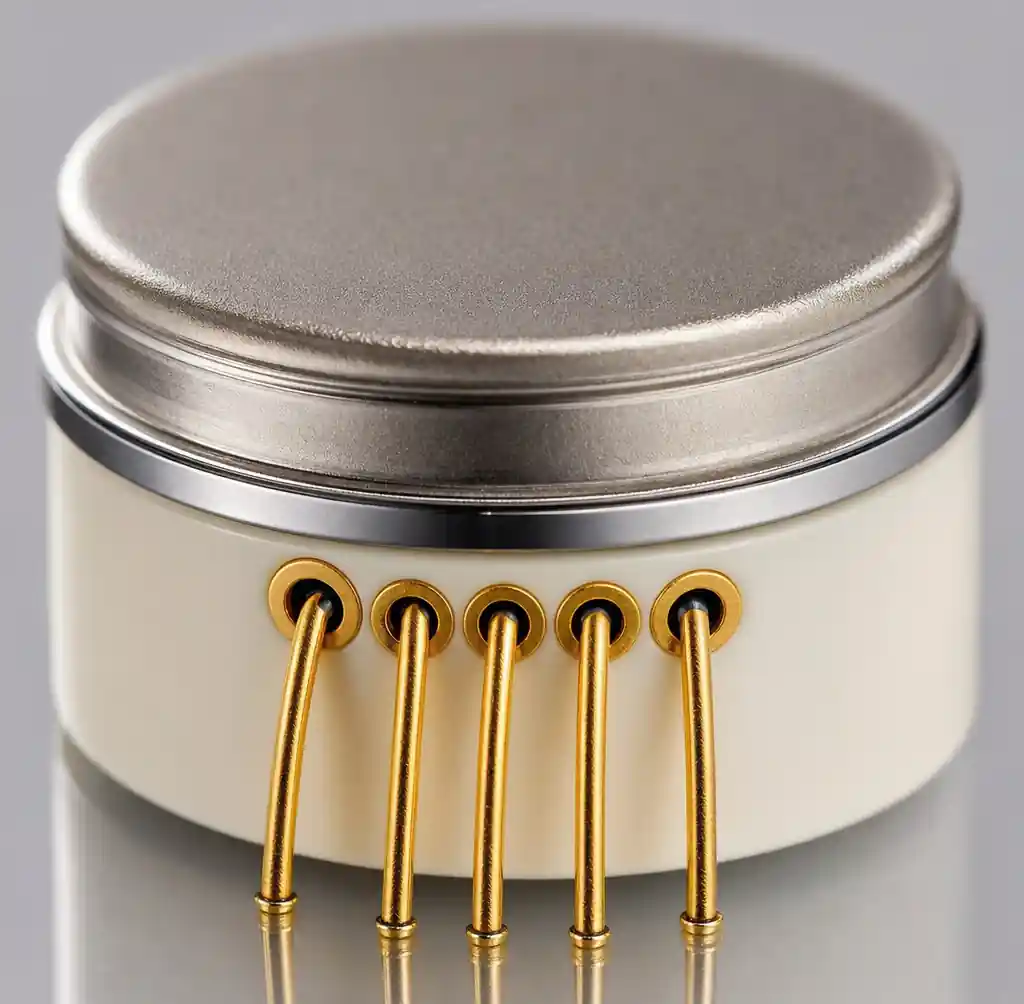
You can use ceramic PCB packages for high-power pulse generators where thermal management is critical. Research shows ceramic housings with gold braze feedthroughs provide optimal biocompatibility and corrosion resistance for cochlear implants and spinal cord stimulators.
Laser Welding for Hermetic Sealing
Laser hermetic welding creates permanent seals joining titanium or stainless steel enclosures without filler materials. Nd:YAG laser systems at 1064 nm wavelength produce focused energy melting base metals along seam lines, forming continuous welds with helium leak rates below 1×10⁻⁹ atm·cc/sec.
Process parameters—laser power (100-400W), pulse duration (0.5-5ms), and overlap (30-50%)—must be optimized preventing thermal damage to internal electronics while ensuring complete penetration. Validation includes helium leak testing, metallography, and accelerated aging in saline at 60-77°C.
Long-Term Reliability Testing
Accelerated Aging Protocols
Accelerated aging in saline is the primary method for predicting implantable PCB longevity. Protocols use phosphate buffered saline (PBS) at elevated temperatures with calculated acceleration factors based on Arrhenius equations.
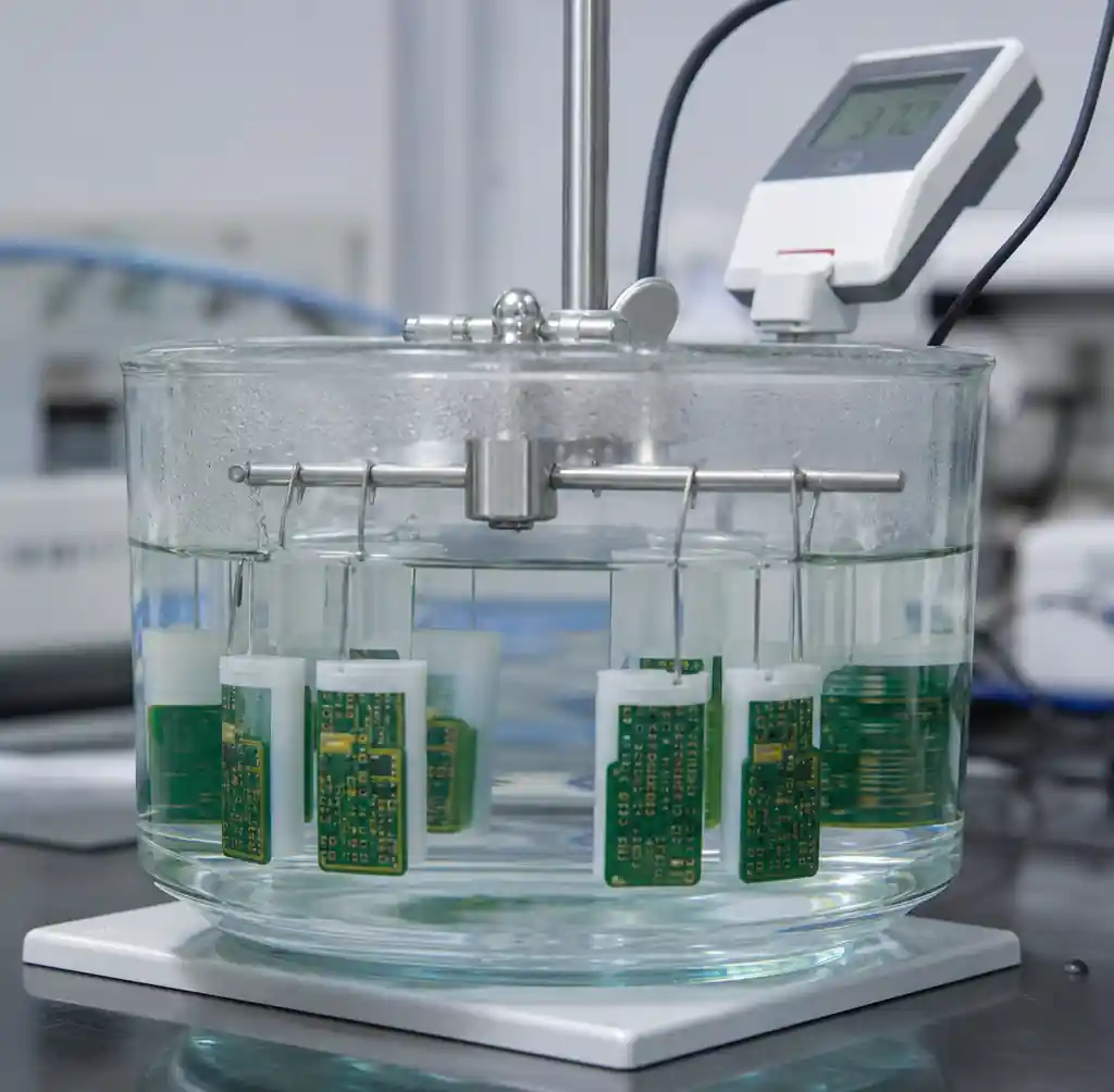
Standard test conditions include temperature at 60°C or 77°C (acceleration factor 4.92× or 8.5× compared to 37°C body temperature), duration of 90-365 days, PBS solution at pH 7.4 with 0.9% NaCl, and monitoring electrical continuity, insulation resistance (>100 MΩ), and functional performance.
Reactive accelerated aging adds 10-20 mM hydrogen peroxide simulating oxidative stress from immune responses. Testing at 77°C for 24 days with H₂O₂ approximates one year of implantation, revealing encapsulation failures not appearing in standard saline aging.
Reliability Performance Data
| Encapsulation Type | Test Condition | Equivalent Lifetime | Failure Mode |
|---|---|---|---|
| Silicone + Parylene | 77°C PBS + H₂O₂, 90 days | 3.7 years | Adhesive delamination |
| Ceramic hermetic | 60°C PBS, 365 days | 18+ years | No failures observed |
| PDMS-coated CMOS | 60°C PBS, 4.3 years | 21+ years | Stable performance |
| Epoxy encapsulation | 77°C PBS, 60 days | 2.4 years | Moisture penetration |
Research shows PDMS-coated devices maintain functionality after 4.3 years of accelerated testing, validating non-hermetic approaches for millimeter-scale neural implants where traditional hermetic packaging is impractical.
PCB Design for Miniaturization
Implantable device miniaturization directly impacts patient comfort and surgical complexity. Modern pacemakers occupy volumes below 10 cm³ compared to 40 cm³ for 1990s devices. You can achieve significant size reduction through HDI PCB technology with laser-drilled microvias and high-density interconnects.
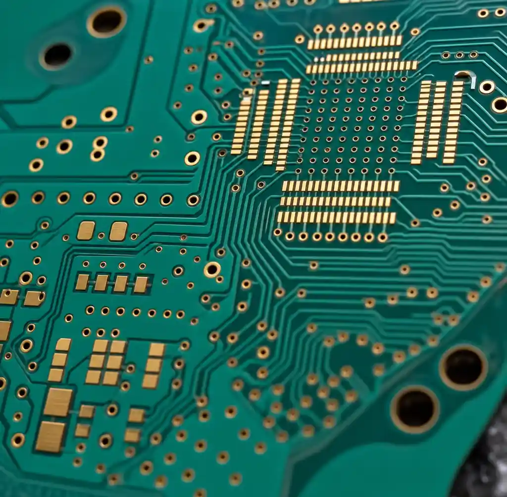
Design techniques include microvia technology with 0.1mm diameter laser-drilled vias enabling dual-side component placement, fine-pitch BGAs at 0.4mm pitch for processors and ASICs, stacked vias using 1+N+1 HDI stackups reducing layer count by 30-40%, embedded passives integrating resistors and capacitors in dielectric layers, and rigid-flex construction eliminating connectors reducing assembly volume by 25-35%.
Research shows every tenth of a millimeter matters for implantable devices, with ultra-compact designs achieving 2-layer PCBs in 12×12mm footprints while maintaining signal integrity for wireless communication.
You should work with manufacturers offering up to 50-layer capabilities and advanced HDI technology for maximum miniaturization. Strategic component placement reduces PCB area while maintaining thermal management—place high-power components near thermal vias connecting to metal core regions or titanium enclosure walls acting as heat sinks.
Power Efficiency and Battery Life
Ultra-Low Power Design
Implantable device power consumption determines battery size, directly impacting device volume. Modern implants operate on tight power budgets ranging from 1-3 mW continuous for neurostimulators to 10-50 µW for passive monitoring devices.
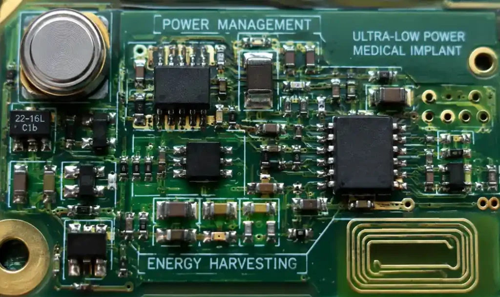
Power optimization includes duty cycling (activating circuits only during measurement or stimulation), power gating (shutting down unused circuit blocks with MOSFET switches), subthreshold operation (running digital logic below threshold voltage at 0.3-0.5V for 10× power reduction), and efficient wireless protocols (BLE 5.0 consuming 5-10 mA for 10 ms bursts versus 20-40 mA continuous for older protocols).
Power management designs achieve peak conversion efficiency above 85% with intrinsic current consumption below 550 nA—critical for battery-powered implants where every microamp of quiescent current shortens device lifetime.
Battery Technologies and Alternatives
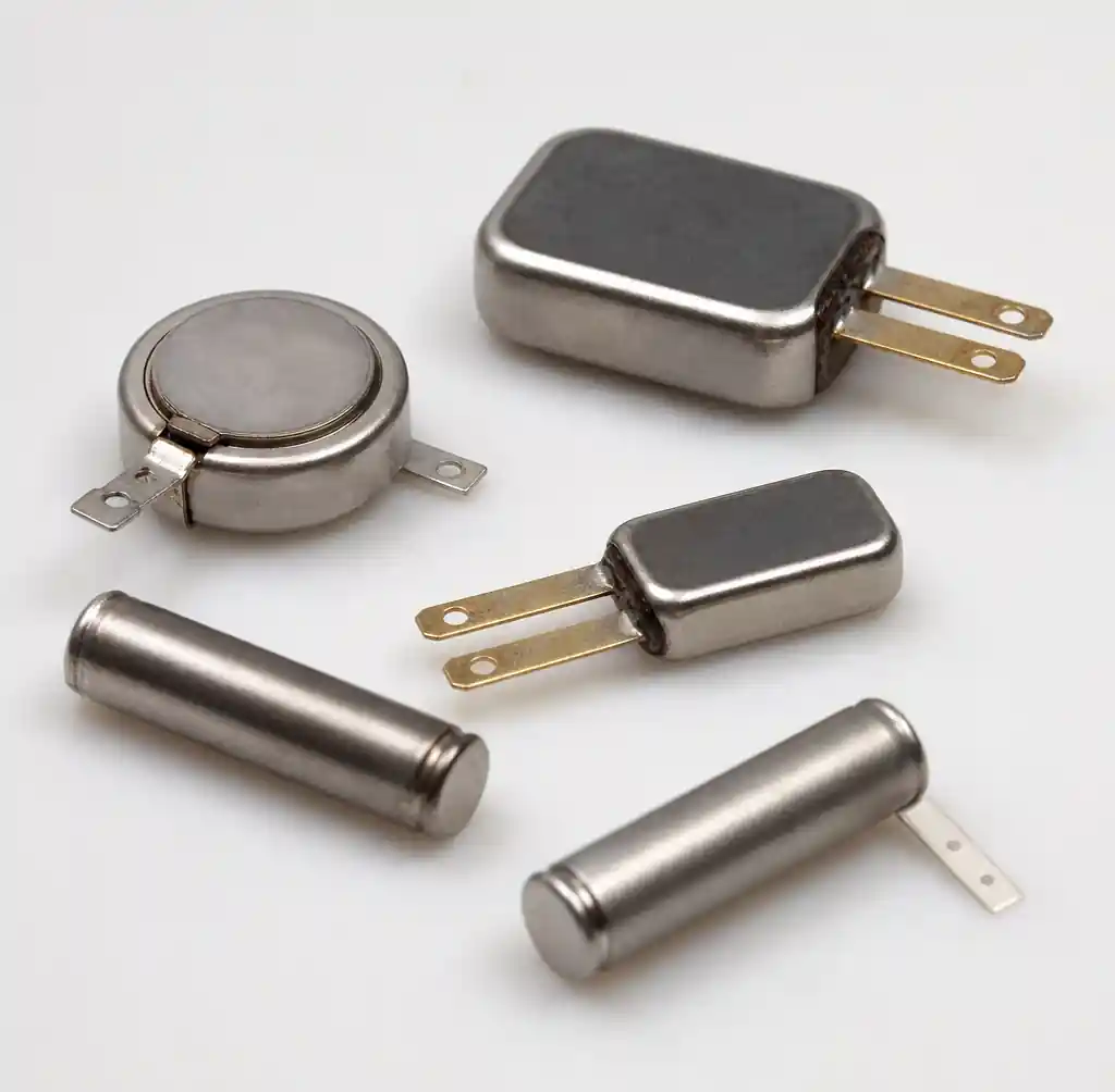
Lithium-ion microbatteries remain the primary energy source for implantable devices due to energy densities reaching 250-350 Wh/kg. Battery selection balances capacity, volume, and safety:
| Battery Type | Energy Density | Cycle Life | Typical Capacity | Applications |
|---|---|---|---|---|
| Li-CFx (Primary) | 350-500 Wh/kg | Single use | 1-3 Ah | Pacemakers (7-10 year life) |
| Li-ion (Rechargeable) | 250-300 Wh/kg | 500-1000 cycles | 50-200 mAh | Neurostimulators, cochlear |
| Solid-state Li | 400-500 Wh/kg | 5000+ cycles | 10-100 mAh | Next-gen (research) |
| Glucose fuel cells | 43 µW/cm² | Continuous | Biofuel | Ultra-low power sensors |
Advances in 3D battery architectures enable continued miniaturization beyond planar design limitations. High-throughput production using stack-punching techniques specifically targets implantable medical devices.
Ceramic-electrolyte glucose fuel cells generate power from body glucose, achieving 43 µW/cm² peak density with high fabrication reliability across 150 devices tested. These eliminate battery replacement surgeries for ultra-low power monitoring applications.
Wireless power transfer systems extend functionality while reducing battery requirements. Inductive coupling at 13.56 MHz or 6.78 MHz transmits power through tissue with 40-60% efficiency at depths up to 5 cm. Design requires SAR compliance below 1.6 W/kg per FCC regulations and tissue heating below 1°C.
Manufacturing Standards and Validation
ISO 13485 and IPC Class 3 Requirements
Medical device PCB manufacturing requires ISO 13485 certification with complete traceability from raw materials through final assembly. IPC Class 3 acceptance criteria specify minimum trace width/spacing at 3/3 mil (75/75 µm) with ±1 mil tolerance, via aspect ratios maximum 12:1 for through-holes, copper thickness uniformity ±20% maximum variation, and 100% electrical testing at 250V minimum.

You should verify manufacturers hold relevant certifications and provide documentation including material certifications, process control records, and dimensional inspection reports for every production lot.
Biocompatibility Testing and Validation
Before clinical use, implantable PCBs undergo comprehensive biological evaluation following ISO 10993 protocols. Testing sequence includes cytotoxicity testing (ISO 10993-5) with L-929 mouse fibroblasts, sensitization testing (ISO 10993-10) using guinea pig maximization, irritation testing via intracutaneous injection, systemic toxicity studies, and implantation testing for up to 26 weeks.
Complete biocompatibility testing for a new implantable PCB design costs $150,000-$300,000 and requires 6-12 months. Beyond biocompatibility, functional qualification includes electrical characterization at -20°C to +60°C, mechanical testing with 1 million+ flex cycles for cardiac applications, hermeticity verification to MIL-STD-883, sterilization compatibility, and EMC testing for MRI immunity per ISO 14117.
Frequently Asked Questions
What is the difference between hermetic and non-hermetic packaging for implantable PCBs?
Hermetic packaging uses glass-to-metal or ceramic-to-metal seals creating vacuum-tight barriers with helium leak rates below 1×10⁻⁸ atm·cc/sec. Non-hermetic approaches use polymer encapsulation (silicone, parylene, epoxy) that slows but does not completely prevent moisture penetration. Hermetic packages provide superior long-term reliability for high-power devices like pacemakers, while non-hermetic methods enable smaller sizes for neural interfaces where miniaturization outweighs the slightly reduced lifespan.
How long do implantable medical device PCBs last inside the body?
Implantable PCB lifespan ranges from 5-7 years for rechargeable neurostimulators to 10-15 years for primary battery pacemakers. Hermetically sealed ceramic packages with proper design achieve 18+ years validated through accelerated aging. Lifespan depends on power consumption, hermetic seal integrity, and biocompatible encapsulation quality. Design verification through accelerated aging at 60-77°C in saline solution predicts real-world performance.
Which PCB materials meet ISO 10993 biocompatibility requirements?
Polyimide (Kapton) substrates, medical-grade FR-4 with validated resin systems, and PEEK materials meet ISO 10993 requirements when properly tested. Surface finishes must use ENIG, hard gold, or platinum/iridium rather than HASL or OSP. All materials require cytotoxicity, sensitization, and irritation testing per ISO 10993-5 and 10993-10. Even standard PCB materials can achieve biocompatibility when encapsulated with validated polymers like medical-grade silicone or parylene coatings.
What are the main failure modes for implantable PCBs?
Primary failure modes include moisture penetration through encapsulation leading to corrosion, hermetic seal breaches allowing bodily fluid ingress, battery depletion, and mechanical failures from cardiac motion or patient activity. Accelerated aging studies show adhesive delamination between encapsulation layers is common within 2-4 years for non-hermetic designs. Proper material selection, hermetic feedthrough design, and validation testing prevent these failures.
Can wireless charging work through body tissue for implanted devices?
Yes, inductive wireless charging at 13.56 MHz or 6.78 MHz penetrates tissue effectively for depths up to 5 cm with 40-60% efficiency. Systems must comply with SAR limits below 1.6 W/kg per FCC regulations and avoid tissue heating beyond 1°C. Commercial cochlear implants and neurostimulators use wireless charging to eliminate battery replacement surgeries. Design requires proper coil geometry, ferrite shielding, and impedance matching for optimal power transfer.
Conclusion
Medical PCBs for implantable devices represent the intersection of advanced electronics manufacturing, materials science, and biomedical engineering. Hermetic sealing through glass-to-metal feedthroughs and ceramic packages provides the foundation for long-term reliability, while ISO 10993 biocompatibility validation ensures patient safety. Engineers must balance miniaturization demands with power efficiency requirements, selecting appropriate HDI PCB technologies and battery solutions delivering 7-15 year operational lifespans.
Accelerated aging protocols in saline solution with reactive oxidative stress simulate decades of implantation, validating both hermetic and polymer-encapsulated designs. Successful implementation requires ISO 13485 certified manufacturing with complete traceability and IPC Class 3 quality standards.
Andwin Circuits offers advanced HDI PCB and rigid-flex PCB manufacturing for medical device applications up to 50 layers with ISO 13485 and IATF 16949 certification. Our medical equipment PCB solutions include design verification support, biocompatibility consulting, and fast turnaround in 7-15 days. Contact us for custom medical PCB manufacturing with complete quality documentation.