
Automotive PCB for ADAS: Radar and Camera Module Design
The global automotive ADAS market is projected to reach $83 billion by 2030, with radar and camera modules accounting for over 60% of sensor deployments. PCB design quality directly determines whether your ADAS system meets ISO 26262 functional safety and AEC-Q qualification standards.
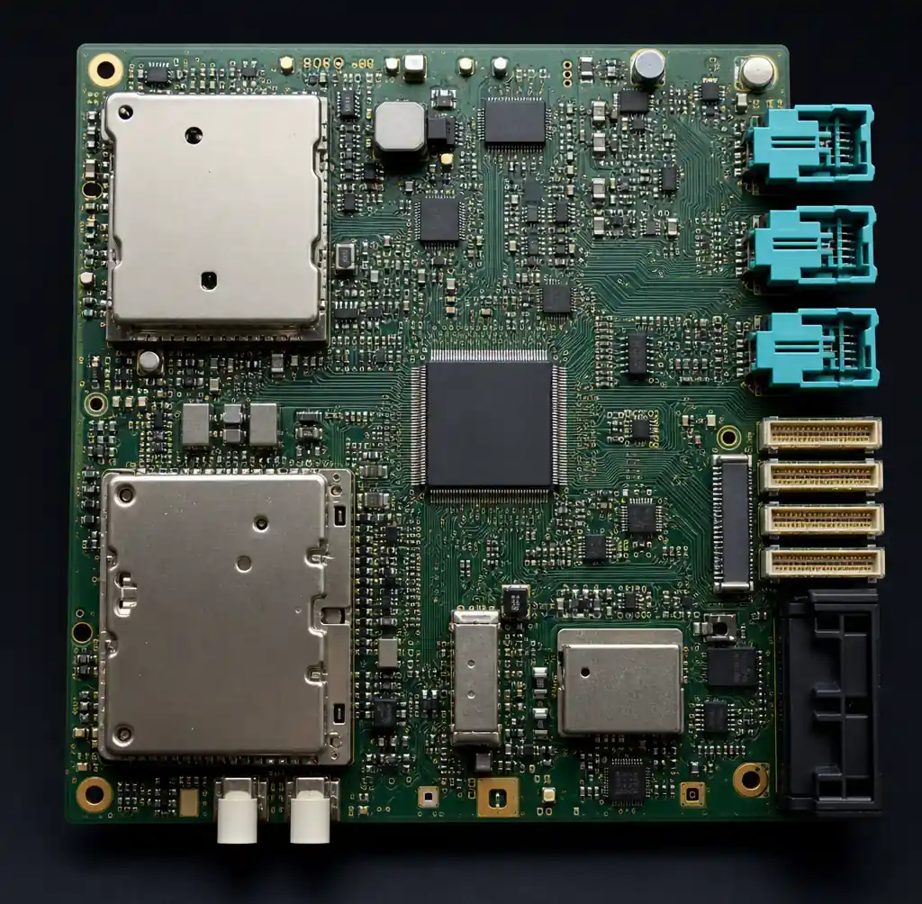
This guide covers critical PCB design requirements for ADAS radar modules operating at 77GHz and camera interface circuits, including material selection, signal integrity, EMI shielding, and automotive reliability testing.
What is ADAS PCB?
An ADAS PCB is a specialized automotive-grade printed circuit board designed to support radar transceivers, camera interfaces, sensor fusion processors, and power management for Advanced Driver Assistance Systems. These boards operate from -40°C to +125°C and must comply with ISO 26262 functional safety standards (typically ASIL-B to ASIL-D levels).
ADAS PCBs integrate 77GHz radar RF sections, high-speed digital interfaces (MIPI CSI-2 for cameras at 1-2 Gbps per lane), and robust power delivery within a compact footprint while providing excellent EMI shielding for automotive electromagnetic compatibility.
77GHz Radar PCB Design Requirements
High-Frequency Material Selection
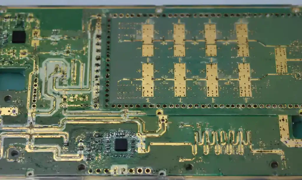
77GHz automotive radar operates in the E-band millimeter-wave spectrum (76-81 GHz). At these frequencies, dielectric constant (Dk) variations of just 0.02 can shift antenna patterns by several degrees.
You should specify Rogers RO4003C (Dk=3.38 ±0.05) and Taconic RF-35 (Dk=3.50 ±0.05) as industry-standard choices. The dissipation factor (Df) must remain below 0.0027 at 77GHz to minimize insertion loss. According to IPC-4103, automotive-grade RF laminates must maintain these properties across -40°C to +150°C with Dk stability better than ±1.5%.
Impedance Control and Antenna Integration
Radar transceivers require 50Ω single-ended transmission lines. At 77GHz, the electrical wavelength in FR-4 is approximately 1.5mm, making small impedance discontinuities problematic.
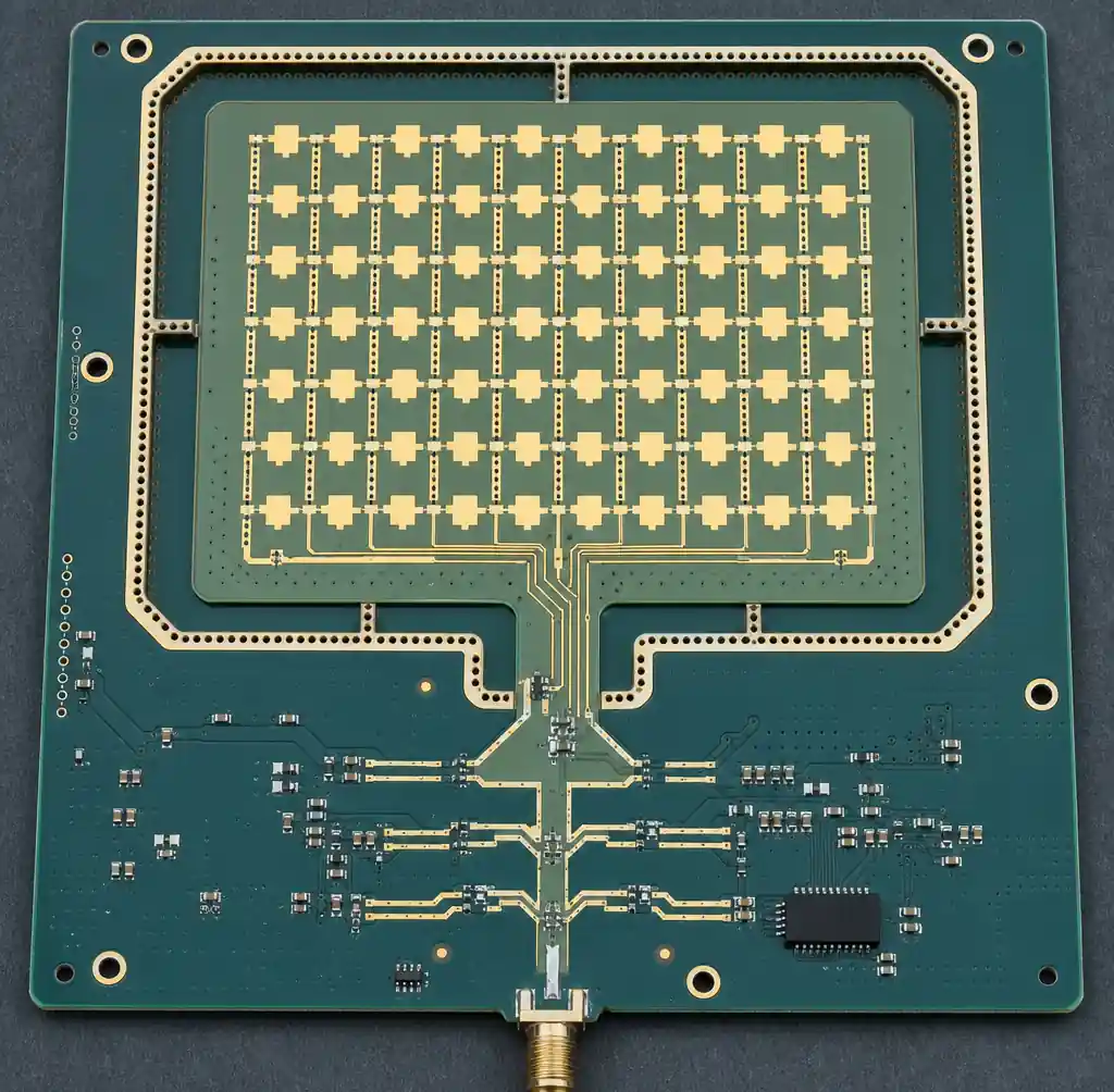
You must specify controlled impedance with ±5% tolerance per IPC-2141 Class 2. Use microstrip or grounded coplanar waveguide (GCPW) with ground vias spaced no more than λ/10 apart (approximately 150μm at 77GHz). Most 77GHz radar modules use patch antenna arrays directly fabricated on the PCB with cavity-backed structures providing 20-30dB isolation between RF and digital layers.
| Parameter | Specification | Standard | Notes |
|---|---|---|---|
| Operating Frequency | 76-81 GHz | ETSI EN 302 858 | Long-range radar |
| PCB Material Dk | 3.38-3.50 ±0.05 | IPC-4103 | Rogers RO4003C/Taconic RF-35 |
| Dissipation Factor | <0.0027 @ 77GHz | Manufacturer spec | Minimize insertion loss |
| Impedance Tolerance | 50Ω ±5% | IPC-2141 Class 2 | RF transmission lines |
| Copper Roughness | <2μm Rz | IPC-4562 | Reduce skin effect loss |
Camera Module Interface Design
MIPI CSI-2 High-Speed Routing
Modern automotive cameras use MIPI CSI-2 interfaces operating at 1-2.5 Gbps per lane. A typical 8-megapixel camera uses 4 data lanes plus one clock lane, all implemented as 100Ω differential pairs.
Route differential pairs with length matching within ±5 mils (±127μm) per lane pair and maintain 100Ω ±10% impedance. Use stripline routing on internal layers for better EMI immunity above 1 Gbps. According to MIPI D-PHY specification, intra-pair skew must not exceed 40ps, translating to approximately 200 mils (5mm) length difference in FR-4.
Power Supply Filtering
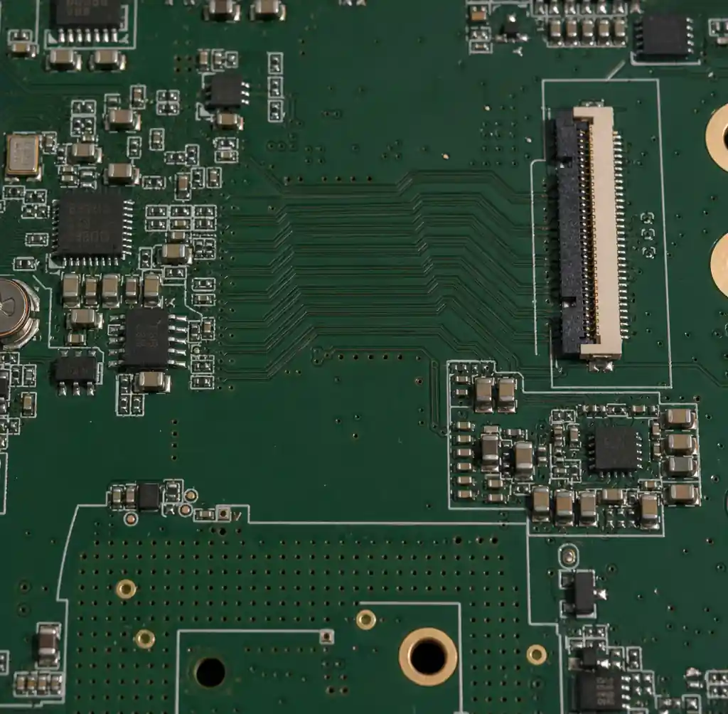
Camera image sensor analog supply (typically 2.8V) needs filtering to below 10mV ripple. Design a π-filter network with 10μF bulk capacitor, ferrite bead (600Ω @ 100MHz), and 1μF ceramic capacitor directly at the camera connector. Place the ferrite bead between bulk and decoupling capacitors with separate analog and digital ground planes.
| Interface Type | Data Rate | Impedance | Standards | Application |
|---|---|---|---|---|
| MIPI CSI-2 | 1-2.5 Gbps/lane | 100Ω differential | MIPI D-PHY v2.1 | Front/surround cameras |
| FPD-Link III | 3.5-4 Gbps | 100Ω differential | TI proprietary | High-resolution cameras |
| Automotive Ethernet | 100M/1000BASE-T1 | 100Ω differential | IEEE 802.3bp/bw | Networked cameras |
Sensor Fusion and Communication Design
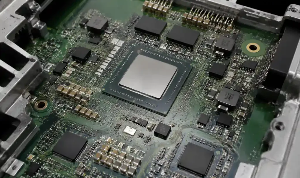
ADAS sensor fusion requires platforms handling real-time data from multiple sensors. Modern ADAS ECUs use automotive-qualified SoCs like NXP S32V or TI TDA4 integrating Arm cores and vision accelerators. These processors generate 5-15W heat requiring thermal management. Design power delivery capable of 10A peak currents with <50mV ripple using 6-8 layer stackup with dedicated power/ground planes.
Automotive Ethernet (100BASE-T1 or 1000BASE-T1) has become standard for inter-sensor communication. Route Ethernet differential pairs as 100Ω impedance-controlled traces with ±5% tolerance and pair-to-pair spacing of at least 3 times trace width.
EMI Shielding and Grounding Strategy
Automotive EMC Requirements
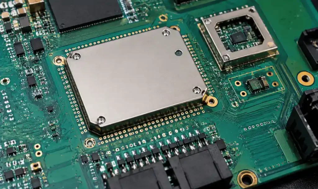
ADAS systems must pass rigorous EMC testing per CISPR 25 (radiated emissions) and ISO 11452 (immunity). Implement multi-layer shielding combining PCB ground planes, RF shield cans over radar transceivers, and conductive gaskets. The shield can must connect to PCB ground at intervals no greater than λ/10 at the highest frequency (typically 6 GHz).
Use star grounding where RF, digital, and analog ground planes connect at a single point near power supply entry. Implement ground plane stitching vias at 5mm spacing. According to IPC-2152, use at least 0.5oz (17μm) copper for internal ground planes and 1oz (35μm) for outer layers.
AEC-Q Qualification and ISO 26262 Compliance
Component and Board Reliability
All components must meet AEC-Q100 (ICs), AEC-Q200 (passives), or AEC-Q101 (discrete semiconductors). Specify Grade 2 (-40°C to +105°C) components for most ADAS applications, or Grade 1 (-40°C to +125°C) for modules near engines.
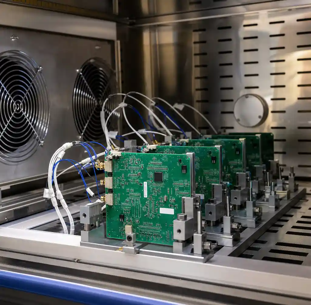
Assembled PCBs must undergo board-level reliability testing. Perform minimum 500 temperature cycles from -40°C to +125°C with 15-minute dwell times per IPC-9701. High-temperature operating life (HTOL) testing at +125°C for 1000 hours confirms design margin for 15-year automotive lifetime.
| Reliability Test | Condition | Duration | Standard | Pass Criteria |
|---|---|---|---|---|
| Temperature Cycling | -40°C to +125°C | 500-1000 cycles | IPC-9701 | No electrical failure |
| HTOL | +125°C powered | 1000 hours | AEC-Q100 | <1% failure rate |
| Thermal Shock | -40°C to +125°C | 200 cycles | JESD22-A106 | No delamination |
| Vibration | 10-2000 Hz, 20G | 12 hours | IEC 60068-2-64 | No mechanical failure |
ISO 26262 Functional Safety
ISO 26262 defines functional safety for automotive electrical systems. ADAS modules are typically ASIL-B to ASIL-D depending on function (lane keeping is ASIL-B, automatic emergency braking is ASIL-D).
Implement hardware safety mechanisms including redundant power supplies, watchdog circuits, and diagnostic coverage. According to ISO 26262 Part 5, achieve at least 90% diagnostic coverage for ASIL-C and 97% for ASIL-D. The target FIT rate for ASIL-D systems is <10 FIT (10 failures per billion hours), achievable through redundancy and extensive diagnostic coverage.
PCB Stackup and Thermal Management
8-Layer Stackup Configuration
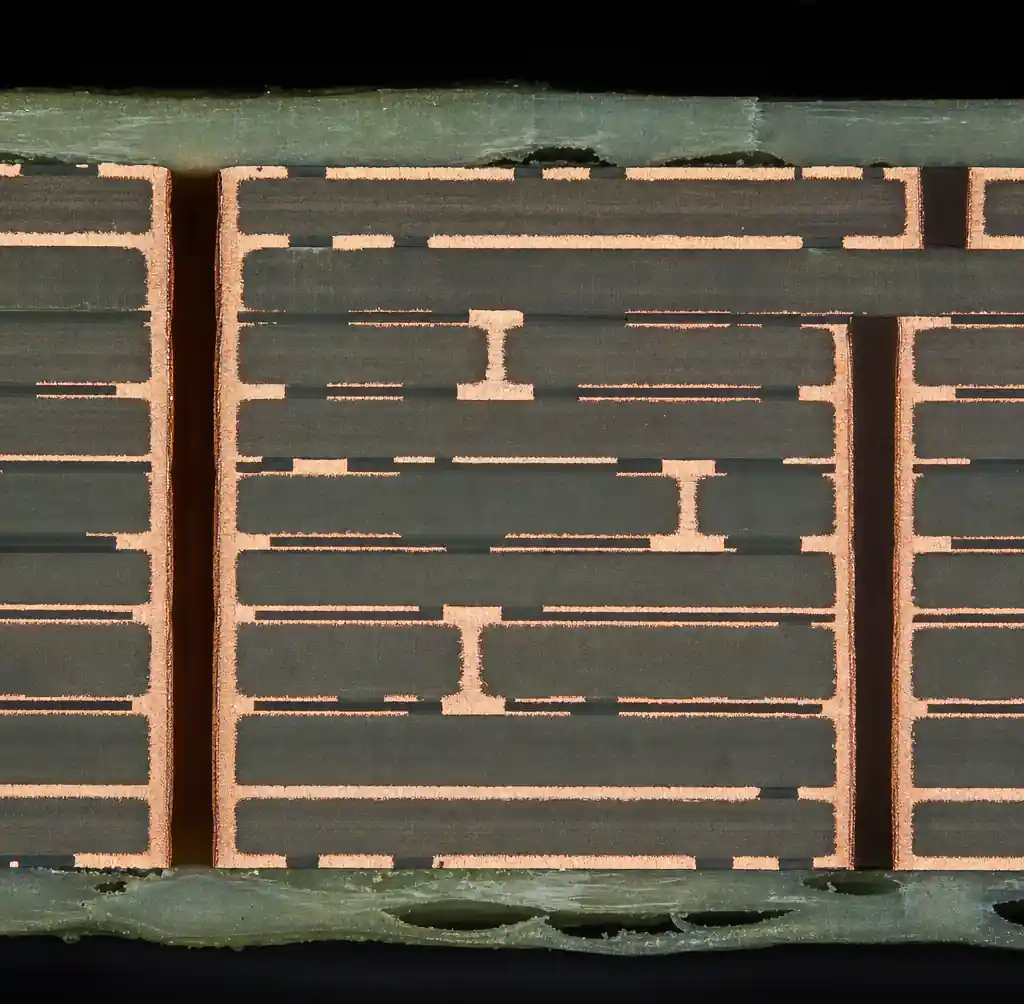
A typical ADAS radar PCB uses 8-layer stackup accommodating 77GHz RF routing, high-speed digital signals, and robust power distribution. Recommended configuration: RF signal (0.5oz) / Ground (1oz) / Digital (0.5oz) / Power (1oz) / Power (1oz) / Digital (0.5oz) / Ground (1oz) / RF/shield (1oz).
Use thicker copper (1-2oz) for power and ground planes to reduce DC resistance. According to IPC-2221, 1oz copper trace 10mm wide can carry 3A continuous current with 10°C temperature rise.
Thermal Via Design
For devices dissipating >2W, implement thermal vias to conduct heat to inner ground planes. Design thermal via arrays with 0.3mm diameter vias spaced on 0.8-1.0mm grid. A 5mm × 5mm QFN thermal pad requires 25-30 thermal vias to achieve thermal resistance below 15°C/W.
Manufacturing Considerations and DFM
Design for Manufacturing
Specify minimum trace widths and spacing of 4/4 mils (100/100μm) for RF sections and 5/5 mils (125/125μm) for digital layers per IATF 16949. Avoid acute angles in traces. Use 45-degree chamfers or curved traces instead of 90-degree corners. Implement teardrops at via-to-trace connections for mechanical strength.
Assembly Process Control
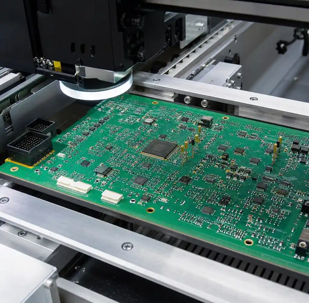
ADAS PCBs require careful assembly because many components are moisture-sensitive (MSL 3 or higher). Maintain proper baking per J-STD-033 before reflow. Use nitrogen reflow (oxygen <100 ppm). Implement automated optical inspection (AOI) after solder paste printing and after reflow. X-ray inspection is mandatory for QFN packages and BGAs.
Selecting an ADAS PCB Manufacturing Partner
When choosing a PCB manufacturer for automotive ADAS, verify they hold IATF 16949 certification and demonstrate experience with high-frequency RF boards. The manufacturer should provide documented process controls per IPC-6012 Class 3.
Andwin Circuits specializes in automotive-grade PCB manufacturing with full IATF 16949 certification. Our facility produces multilayer PCBs up to 50 layers with controlled impedance testing. We support RF materials including Rogers and Taconic laminates and provide fast turnaround in 7 days for prototypes.
For automotive PCB applications requiring impedance control, reference our guide on controlled impedance PCB design. Our automotive PCB requirements guide covers complete quality system requirements.
FAQ
What materials are best for 77GHz automotive radar PCBs?
Rogers RO4003C (Dk=3.38) and Taconic RF-35 (Dk=3.50) are industry-standard materials because they provide stable dielectric properties from -40°C to +150°C with dissipation factors below 0.0027 and tight Dk tolerance (±0.05) critical for antenna performance.
How do ADAS PCBs differ from standard automotive PCBs?
ADAS PCBs support millimeter-wave RF circuits at 77GHz, high-speed camera interfaces at multi-gigabit rates, and meet ISO 26262 functional safety requirements. They require specialized RF materials, controlled impedance design, and qualification to higher reliability levels (500-1000 temperature cycles vs 200 for standard automotive).
What is the typical lead time for ADAS PCB prototypes?
Standard lead time is 10-15 days due to specialized RF materials. Andwin Circuits offers fast-turn service with 7-day delivery for urgent projects. Production volumes require 3-4 weeks including material procurement and reliability testing.
How is ISO 26262 compliance verified at the PCB level?
ISO 26262 compliance is verified through design reviews demonstrating adequate diagnostic coverage, hardware safety mechanisms, and FIT rate calculations. You must provide evidence of redundant power supplies, watchdog circuits, and fault detection. Hardware testing includes FMEA analysis, component derating verification, and stress testing beyond normal operating conditions.
What layer count is recommended for ADAS radar and camera modules?
An 8-10 layer stackup is recommended for integrated ADAS modules combining radar and camera interfaces. This provides separate RF layers for 77GHz routing, dedicated ground planes for shielding, stripline layers for high-speed digital signals, and robust power distribution.
Conclusion
Automotive PCB design for ADAS radar and camera modules requires specialized expertise in high-frequency RF design, high-speed digital interfaces, and automotive reliability standards. Success requires careful material selection, precise impedance control, comprehensive EMI shielding, and rigorous qualification per AEC-Q and IATF 16949 standards.
If you need high-quality automotive PCBs for ADAS applications, Andwin Circuits offers advanced manufacturing with IATF 16949 certification. Contact us today for custom automotive PCB solutions and competitive pricing.