
Methods for Adding Process Edges and MARK Points in PCB Design
Abstract
In printed circuit board (PCB) design, process edges (also called breakaway tabs or rails) and fiducial markers (MARK points) are essential for manufacturing and assembly. Process edges provide mechanical support during fabrication, while MARK points ensure accurate component placement during surface mount technology (SMT) assembly. This article discusses the purpose, design guidelines, and implementation methods for process edges and MARK points in PCB design, providing a comprehensive guide for engineers and designers.
1. Introduction
PCBs undergo multiple stages during manufacturing, including fabrication, assembly, and testing. To ensure smooth production, designers must incorporate process edges and fiducial markers. Process edges are additional strips of material added along the PCB’s perimeter to facilitate handling, while fiducial markers are reference points used by pick-and-place machines for precise component alignment.
This article explores the following aspects:
- The importance of process edges and MARK points
- Design guidelines for process edges
- Types and placement of fiducial markers
- Implementation in PCB design software
- Common mistakes and troubleshooting
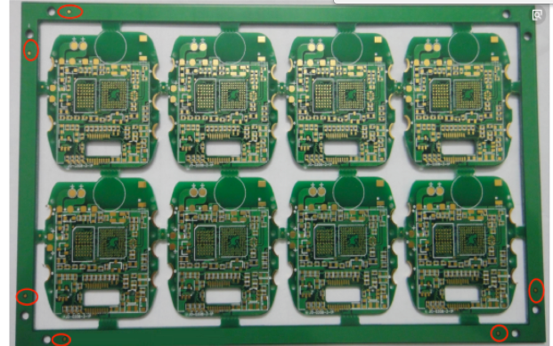
2. Process Edges in PCB Design
2.1 Purpose of Process Edges
Process edges serve several functions:
- Mechanical Support: Prevents PCB warping during fabrication and assembly.
- Conveyor Belt Handling: Ensures smooth movement through automated assembly lines.
- Panelization Aid: Facilitates depaneling (breaking PCBs from panels after assembly).
- Tooling Hole Placement: Provides space for mounting holes used in assembly fixtures.
2.2 Design Guidelines for Process Edges
When adding process edges, follow these best practices:
2.2.1 Width and Thickness
- A typical process edge width is 5-10mm, depending on PCB size and assembly requirements.
- The edge should match the PCB thickness to avoid warping.
2.2.2 V-Grooves and Tab Routing
- V-grooves (scored lines) allow easy depaneling but require a straight edge.
- Tab routing uses small connecting tabs (typically 2-4mm wide) with perforations for breakaway.
2.2.3 Tooling and Fiducial Placement
- Place tooling holes (3.0mm diameter recommended) in the process edges for alignment.
- Ensure fiducial markers are included in the process edge if needed.
2.2.4 Clearance Considerations
- Keep critical traces and components at least 5mm away from the process edge to avoid damage during depaneling.
2.3 Implementing Process Edges in CAD Software
Most PCB design tools (Altium Designer, KiCad, Eagle) allow process edge definition:
- Define the Board Outline: Draw the main PCB shape.
- Add Process Edge Layers: Use mechanical layers to mark process edges.
- Specify Depaneling Method: Add V-cut or tab routing indicators.
- Generate Gerber Files: Include process edges in fabrication outputs.
3. Fiducial MARK Points in PCB Design
3.1 Purpose of Fiducial Markers
Fiducial markers (MARK points) are reference points used by automated assembly machines to:
- Align PCBs for accurate component placement.
- Compensate for PCB Stretch or Shrinkage during manufacturing.
- Improve SMT Assembly Precision, especially for fine-pitch components.
3.2 Types of Fiducial Markers
There are three main types:
3.2.1 Global Fiducials
- Placed on process edges or corners of the PCB.
- Used for coarse alignment of the entire board.
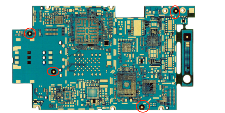
3.2.2 Local Fiducials
- Positioned near high-precision components (e.g., BGAs, QFNs).
- Ensures precise placement of specific parts.
3.2.3 Panel Fiducials
- Used in multi-PCB panels for alignment before depaneling.
3.3 Design Guidelines for Fiducial Markers
3.3.1 Shape and Size
- Recommended Shape: Solid round copper pads (non-solder-masked).
- Diameter: Typically 1.0mm to 3.0mm (larger for global fiducials).
- Clearance: Ensure a 2mm solder mask opening around the fiducial.
3.3.2 Placement Rules
- Global Fiducials: At least 3 points (preferably diagonally opposite corners).
- Local Fiducials: Place symmetrically near critical components.
- Avoid Obstructions: No silkscreen or components should block fiducials.
3.3.3 Contrast Requirements
- Ensure high contrast between the fiducial and background (e.g., bare copper vs. green solder mask).
3.4 Implementing MARK Points in PCB Design
- Add Fiducial Pads: Place copper circles on a dedicated layer.
- Define Solder Mask Openings: Prevent solder mask coverage.
- Verify Machine Compatibility: Check assembly equipment requirements.
4. Common Mistakes and Troubleshooting
4.1 Process Edge Issues
- Insufficient Width: Leads to PCB bending during handling.
- Improper Depaneling Design: Causes board damage during separation.
- Missing Tooling Holes: Results in misalignment during assembly.
4.2 Fiducial Marker Problems
- Low Contrast: Machine vision systems fail to detect fiducials.
- Incorrect Placement: Causes misalignment of components.
- Silkscreen Overlap: Obstructs fiducial recognition.
5. Conclusion
Process edges and fiducial markers are critical for PCB manufacturability and assembly accuracy. By following industry-standard design guidelines, engineers can ensure smooth fabrication and high-quality SMT assembly. Proper implementation in CAD tools and collaboration with manufacturers further enhances PCB reliability.
Key Takeaways:
- Process edges should be 5-10mm wide with proper depaneling features.
- Fiducial markers must have high contrast and correct placement.
- Always verify design rules with fabrication and assembly partners.
By adhering to these methods, PCB designers can optimize their layouts for efficient and error-free production.