
PCB Chip Package Soldering Methods and Process Flow
Abstract
This paper provides a comprehensive overview of printed circuit board (PCB) chip package soldering methods and their detailed process. With the continuous miniaturization and performance enhancement of electronic devices, advanced soldering techniques have become increasingly critical in electronics manufacturing. The article examines various soldering technologies including reflow soldering, wave soldering, selective soldering, and manual soldering, while analyzing their respective process flows, advantages, limitations, and application scenarios. Special attention is given to surface mount technology (SMT) soldering processes and through-hole technology (THT) soldering methods. The paper also discusses quality control measures, common defects, and inspection techniques throughout the soldering process.
1. Introduction
Printed circuit board assembly represents one of the most crucial stages in electronics manufacturing, with chip package soldering quality directly impacting product reliability and performance. As electronic components continue to evolve toward smaller sizes, higher densities, and greater functionality, soldering techniques must correspondingly advance to meet these challenges. Modern PCB soldering encompasses a variety of methods suitable for different component types, package forms, and production requirements.
This article systematically introduces mainstream PCB chip package soldering methods, detailing their工艺流程 while providing technical references for electronics manufacturing professionals. Understanding these soldering techniques enables manufacturers to select appropriate methods based on product characteristics, thereby improving production efficiency and product quality.
2. Surface Mount Technology (SMT) Soldering Methods
2.1 Reflow Soldering Process
Reflow soldering stands as the predominant method for surface mount device (SMD) assembly, consisting of four main phases:
2.1.1 Solder Paste Printing
The initial stage involves precisely depositing solder paste onto PCB pads using a stencil printer. Key parameters include:
- Squeegee pressure (typically 5-15 kg)
- Printing speed (20-80 mm/s)
- Separation speed (0.1-3 mm/s)
- Stencil alignment accuracy (±25 μm)
2.1.2 Component Placement
High-speed pick-and-place machines accurately position components on solder paste deposits with placement accuracy reaching ±30 μm for chip components and ±50 μm for fine-pitch devices.
2.1.3 Reflow Profile
The temperature profile critically determines soldering quality, typically comprising four zones:
- Preheat zone (20-150°C, 60-120s): Gradually heats assembly to activate flux
- Soak zone (150-180°C, 60-90s): Equalizes temperature across components
- Reflow zone (183-220°C, 40-60s): Peak temperature melts solder particles
- Cooling zone: Controlled solidification forms reliable joints
2.1.4 Inspection and Cleaning
Automated optical inspection (AOI) verifies solder joint quality before final cleaning removes flux residues.
2.2 Variations of Reflow Soldering
- Vapor Phase Soldering: Utilizes heat transfer fluids for uniform temperature distribution
- Infrared Reflow: Employs IR radiation for heating, suitable for low-mass assemblies
- Convection Reflow: Forced hot air circulation ensures consistent heating
3. Through-Hole Technology (THT) Soldering Methods
3.1 Wave Soldering Process
Traditional method for through-hole components featuring these stages:
3.1.1 Flux Application
- Spray fluxing: Most common method (20-50 μm coating thickness)
- Foam fluxing: For simple boards
- Selective fluxing: For mixed-technology boards
3.1.2 Preheating
- Activates flux (80-110°C)
- Minimizes thermal shock (90-120s duration)
3.1.3 Wave Contact
- Primary wave (chip wave): Turbulent wave penetrates high-density areas
- Secondary wave (laminar wave): Forms smooth fillets (contact time 2-5s)
3.1.4 Cooling
Forced air cooling solidifies joints at 2-4°C/s rate
3.2 Selective Soldering
Hybrid approach combining wave and reflow principles:
- Programmable nozzle targets specific through-hole components
- Suitable for mixed SMT/THT assemblies
- Minimizes thermal stress on nearby SMDs
4. Specialized Soldering Techniques
4.1 Laser Soldering
- Localized heating (spot size 0.2-2mm)
- Precise energy control (10-100W)
- Applications: Sensitive components, repair work
4.2 Induction Soldering
- Electromagnetic field heating
- Rapid thermal cycles (5-20s)
- Suitable for large metallic components
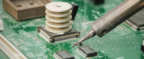
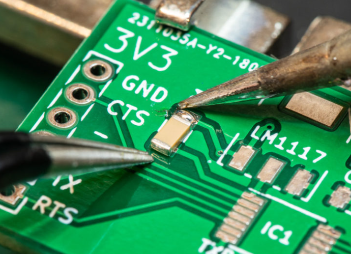
4.3 Manual Soldering
Remains essential for:
- Prototype development
- Rework operations
- Low-volume production
Technique highlights:
- Iron temperature: 300-400°C
- Contact time: <3s per joint
- Solder wire diameter: 0.3-1.0mm
5. Process Flow Comparison
| Parameter | Reflow Soldering | Wave Soldering | Selective Soldering |
|---|---|---|---|
| Component Types | SMD | THT | Mixed |
| Thermal Profile | Controlled | Less Controlled | Targeted |
| Throughput | High (20k+/hr) | Medium (5k/hr) | Low (1k/hr) |
| Defect Rate | 50-200 PPM | 100-500 PPM | 50-300 PPM |
| Equipment Cost | $100k-$1M | $50k-$300k | $150k-$500k |
6. Quality Control and Inspection
6.1 Common Defects
- Solder Bridges: Excessive solder causing shorts
- Tombstoning: Component lifting due to uneven heating
- Voiding: Gas entrapment in joints (acceptance <25% void area)
- Cold Joints: Incomplete metallurgical bonding
6.2 Inspection Methods
- Automated Optical Inspection (AOI): 2D/3D imaging (10-50μm resolution)
- X-Ray Inspection: For BGA and hidden joints (5-20μm resolution)
- Electrical Testing: Continuity and isolation checks
- Cross-Sectioning: Destructive analysis for process validation
7. Emerging Trends
- Low-Temperature Soldering: Sn-Bi alloys (138°C melting point)
- Transient Liquid Phase Soldering: Forms high-melt intermetallics
- Nanoparticle Solder Pastes: Enhanced wetting characteristics
- Environmentally Friendly Fluxes: Halogen-free formulations
8. Conclusion
PCB chip package soldering encompasses diverse methodologies tailored to specific assembly requirements. As packaging technologies advance toward finer pitches (0.3mm pitch becoming standard) and 3D configurations, soldering processes must continuously evolve. Proper selection and optimization of soldering techniques significantly impact manufacturing yield, with leading electronics manufacturers achieving defect rates below 100 parts per million (PPM) through rigorous process control.
Future developments will likely focus on adaptive soldering systems incorporating real-time thermal monitoring and closed-loop process adjustment, further enhancing soldering precision and reliability in increasingly complex electronic assemblies.