Multi-Layer Ceramic PCB Material Stackup: Optimizing for 2-12 Layer Designs
Table of Contents
- Introduction: What This Ceramic PCB Stackup Guide Covers
- Understanding Ceramic PCB Materials and Their Unique Properties
- Layer Count Selection: 2-Layer to 12-Layer Design Considerations
- Critical Stackup Parameters for Ceramic PCB Design
- Material Selection: LTCC vs HTCC for Multi-Layer Applications
- Design Rules and Manufacturing Constraints by Layer Count
- Thermal Management and Via Design in Ceramic Stackups
- FAQ
- Conclusion and Design Recommendations
1. Introduction: What This Ceramic PCB Stackup Guide Covers
Multi-layer ceramic PCBs represent a specialized subset of advanced circuit board technology, primarily used in high-reliability applications where standard FR4 materials cannot meet thermal, electrical, or environmental requirements. This guide addresses the stackup design challenges specific to ceramic substrates ranging from 2 to 12 layers, focusing on material selection, impedance control, and manufacturability constraints that differ significantly from conventional organic PCBs.
Unlike FR4-based multilayer boards, ceramic PCBs—whether Low-Temperature Co-fired Ceramic (LTCC) or High-Temperature Co-fired Ceramic (HTCC)—require fundamentally different design approaches due to their material properties, firing processes, and via formation methods. The dielectric constant (Dk) of ceramic materials typically ranges from 4.0 to 9.8 depending on composition, compared to FR4’s 4.2-4.5, which directly impacts trace geometry calculations for controlled impedance designs.
This article targets hardware design engineers and RF engineers working on applications such as automotive radar modules, aerospace avionics, high-power LED substrates, and millimeter-wave communication systems. You’ll learn how to optimize layer stackup configuration, select appropriate ceramic materials based on thermal and electrical requirements, and avoid common DFM pitfalls that can result in costly redesigns or yield issues during the co-firing process.
2. Understanding Ceramic PCB Materials and Their Unique Properties
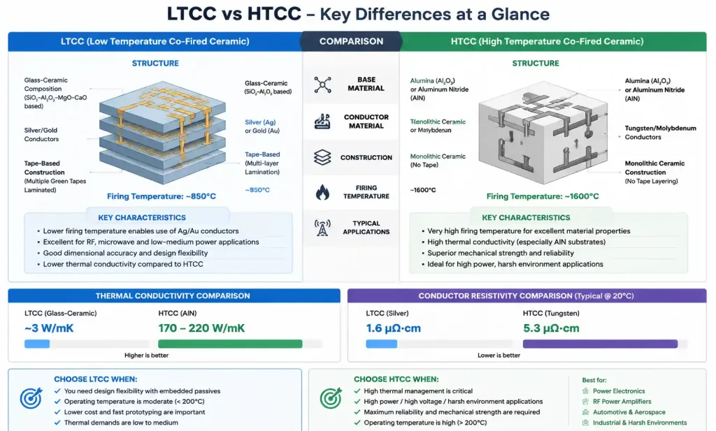
Ceramic PCB materials fundamentally differ from organic substrates in their composition, processing, and performance characteristics. The two primary ceramic technologies—LTCC and HTCC—each offer distinct advantages depending on application requirements.
LTCC materials typically consist of glass-ceramic composites that can be co-fired at temperatures between 850°C and 900°C. This lower firing temperature allows the use of high-conductivity metals like silver, gold, or copper as conductor materials, making LTCC ideal for RF and microwave applications requiring low loss tangent (Df typically 0.001-0.005). Common LTCC materials include DuPont 951 Green Tape (Dk = 7.8 at 3 GHz) and Ferro A6M (Dk = 5.9 at 10 GHz).
HTCC substrates use pure alumina (Al₂O₃) or aluminum nitride (AlN) ceramics that require firing at temperatures exceeding 1600°C. This high-temperature process limits conductor options to refractory metals like tungsten or molybdenum, which exhibit higher resistivity than silver but provide superior thermal performance. Alumina HTCC offers thermal conductivity around 24-35 W/mK, while AlN HTCC reaches 170-220 W/mK—comparable to copper—making it essential for high-power LED modules and power electronics where heat dissipation is critical.
The material choice impacts every aspect of stackup design. LTCC’s tape-based construction allows for embedded passive components and complex via structures including stacked and staggered vias, while HTCC’s punched-via process limits design flexibility but provides better mechanical strength and higher thermal conductivity. The coefficient of thermal expansion (CTE) also differs significantly: LTCC materials typically range from 4-8 ppm/°C, while alumina HTCC is around 6.8 ppm/°C and AlN HTCC approximately 4.5 ppm/°C. These CTE values must be considered when designing solder joints to silicon dies or when mounting on metal substrates.
| Material Type | Dk (at 10 GHz) | Df | Thermal Conductivity (W/mK) | CTE (ppm/°C) | Firing Temp (°C) | Typical Conductor |
|---|---|---|---|---|---|---|
| LTCC (DuPont 951) | 7.8 | 0.006 | 3.0 | 5.8 | 850 | Ag, Au, Cu |
| LTCC (Ferro A6M) | 5.9 | 0.002 | 2.5 | 6.2 | 875 | Ag, Au |
| HTCC Alumina (96%) | 9.8 | 0.0003 | 24-35 | 6.8 | 1600 | W, Mo |
| HTCC AlN | 8.8 | 0.0010 | 170-220 | 4.5 | 1800 | W, Mo |
This material comparison demonstrates why LTCC dominates RF applications where low Df is critical, while HTCC AlN is preferred for high-power applications requiring thermal management. When designing your stackup, the material selection should precede layer count determination, as manufacturing constraints differ significantly between LTCC and HTCC processes.
3. Layer Count Selection: 2-Layer to 12-Layer Design Considerations
Selecting the optimal layer count for ceramic PCB stackup requires balancing electrical performance requirements, thermal management needs, manufacturing complexity, and cost constraints. Unlike FR4 boards where adding layers primarily addresses routing density, ceramic PCB layer decisions must account for via formation limitations, co-firing yield, and thermal path optimization.
For 2-4 layer ceramic designs, the primary driver is typically cost reduction and simplified manufacturing. Two-layer LTCC or HTCC substrates are suitable for basic RF matching networks, LED driver circuits, or simple power modules where signal integrity requirements are modest and power dissipation can be managed through surface-mounted heat sinks. The via aspect ratio in 2-layer designs typically ranges from 1:1 to 3:1, allowing larger via diameters (0.15-0.25mm for LTCC, 0.30-0.50mm for HTCC) that improve manufacturing yield during the via-fill process.
Four-layer stackups represent a practical middle ground for many applications. This configuration allows a dedicated ground plane, power distribution layer, and two signal layers—sufficient for moderate-complexity RF circuits or mixed-signal designs. In LTCC processes, 4-layer designs can incorporate buried resistors and capacitors, reducing component count and improving high-frequency performance by minimizing parasitic inductance.
Six to eight-layer stackups are common in millimeter-wave applications, phased array antennas, and automotive radar modules operating at 24 GHz or 77 GHz. These designs leverage multiple signal layers to implement stripline configurations for optimal impedance control and electromagnetic shielding. The increased layer count allows tighter ground-signal-ground (G-S-G) structures that reduce crosstalk and improve return loss performance. Manufacturing complexity increases significantly beyond 6 layers due to layer-to-layer alignment tolerances; LTCC processes typically maintain registration accuracy within ±75 μm across 6 layers but may exceed ±100 μm at 10-12 layers.
Ten to twelve-layer ceramic stackups are reserved for extremely complex RF front-end modules, System-in-Package (SiP) designs, or high-density power distribution networks. At this layer count, thermal management becomes paramount. The internal conductor layers act as thermal spreading planes, and via arrangement must be optimized not just for electrical connectivity but also for heat transfer. Manufacturing yield decreases with layer count due to cumulative risks during tape stacking, via alignment, and co-firing shrinkage control.
| Layer Count | Typical Applications | Via Aspect Ratio | Manufacturing Yield | Relative Cost |
|---|---|---|---|---|
| 2 Layers | Basic RF matching, simple LED drivers | 1:1 to 3:1 | 98-99% | 1.0× |
| 4 Layers | RF transceivers, mixed-signal modules | 3:1 to 5:1 | 95-98% | 1.8-2.2× |
| 6 Layers | Millimeter-wave circuits, radar modules | 5:1 to 7:1 | 90-95% | 3.0-3.8× |
| 8 Layers | Phased array elements, complex SiP | 7:1 to 9:1 | 85-92% | 4.5-5.5× |
| 10-12 Layers | Advanced RF front-end, high-power distribution | 9:1 to 12:1 | 80-88% | 6.5-8.0× |
The cost scaling is non-linear primarily due to yield loss and increased process complexity. When determining layer count, evaluate whether your routing density and impedance control requirements justify the manufacturing complexity. In many cases, a 6-layer LTCC design with careful layer planning can achieve similar performance to an 8-layer design at significantly lower cost and higher yield.
4. Critical Stackup Parameters for Ceramic PCB Design
Effective ceramic PCB stackup design requires precise control over several interdependent parameters that directly affect electrical performance, thermal management, and manufacturing yield. Unlike FR4 stackups where prepreg thickness can be adjusted during lamination, ceramic layer thicknesses are fixed by the tape or substrate specifications, making upfront design calculations critical.
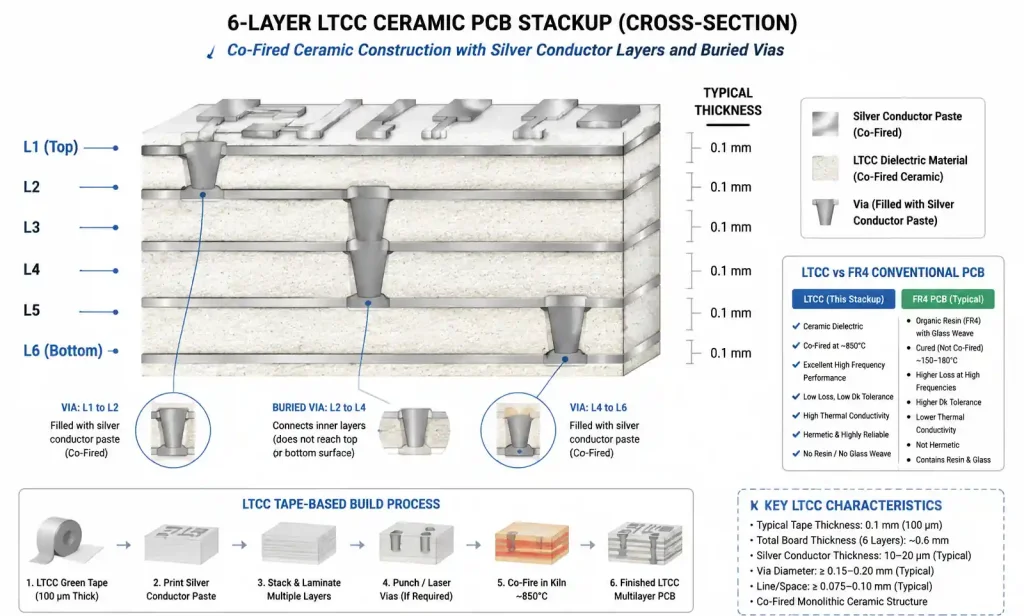
Dielectric layer thickness in LTCC designs is determined by the green tape specification. Common LTCC tapes are available in fired thicknesses of 0.040mm, 0.065mm, 0.100mm, and 0.254mm. Multiple tapes can be stacked to achieve custom thicknesses, but each tape boundary introduces a potential delamination risk during co-firing. For controlled impedance designs, single-tape dielectric layers are preferred when possible. HTCC substrates offer less flexibility, with standard layer thicknesses typically 0.25mm, 0.38mm, or 0.635mm per layer.
Conductor thickness in LTCC processes depends on screen-printing parameters and metal paste formulation. Silver conductors typically achieve 8-12 μm fired thickness per print pass, while gold conductors yield 6-10 μm. For low-resistance power distribution or ground planes, multiple print passes can increase thickness to 20-30 μm, though this increases manufacturing cost and requires careful process control to avoid conductor sagging during firing. HTCC conductor thickness is generally thinner, ranging from 5-10 μm for tungsten or molybdenum metallization.
Impedance calculation for ceramic substrates must account for the material’s higher dielectric constant compared to FR4. For a 50-ohm microstrip line on LTCC material with Dk = 7.8, the required trace width is significantly narrower than on FR4. Using the simplified microstrip formula, a 0.1mm dielectric thickness requires approximately 0.15mm trace width for 50 ohms—compared to 0.18mm on FR4. This narrower geometry increases sensitivity to manufacturing variations in line width and dielectric thickness.
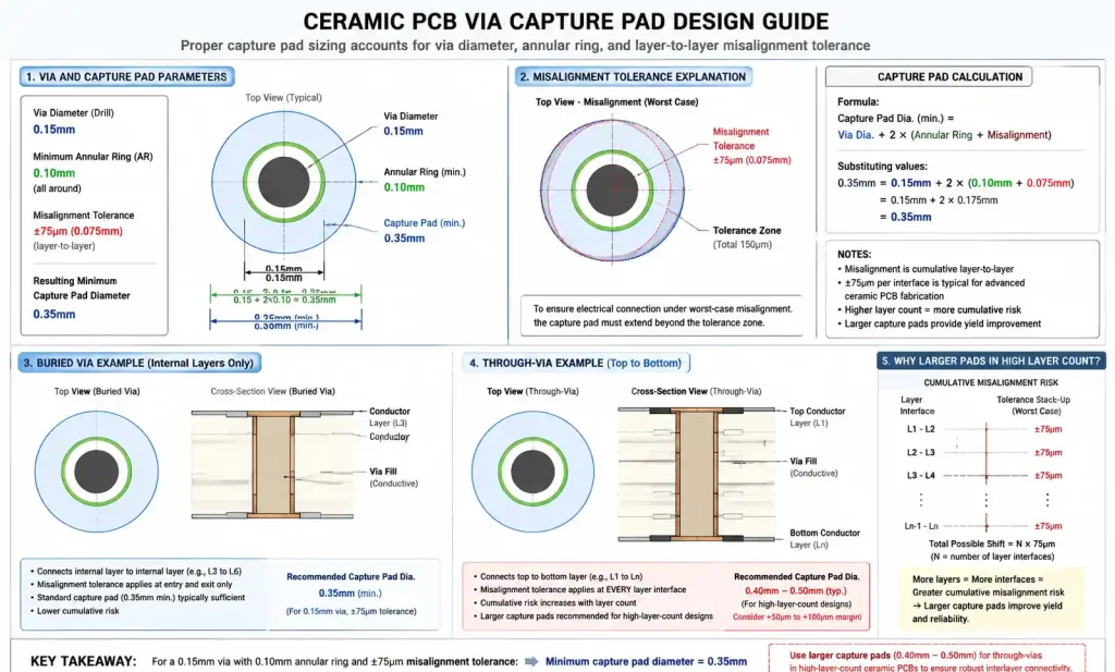
Via design in ceramic stackups presents unique challenges. LTCC vias are formed by punching holes in unfired tape and filling with conductive paste, while HTCC vias are laser-drilled or mechanically punched before metallization. Via diameter must balance electrical performance (lower inductance favors larger vias) against mechanical reliability (smaller vias reduce stress concentration). Minimum via diameter is typically 0.10mm for LTCC and 0.15mm for HTCC, though 0.15mm and 0.25mm respectively are recommended for high-yield production.
Via capture pad diameter should maintain at least 0.10mm annular ring after accounting for layer-to-layer misalignment. With typical LTCC alignment accuracy of ±75 μm, a 0.15mm via requires a minimum 0.35mm capture pad (0.15mm via + 2 × 0.10mm annular ring). Buried vias (connecting internal layers only) can use smaller capture pads than through-vias that connect to surface pads.
| Stackup Parameter | LTCC Range | HTCC Range | Design Impact |
|---|---|---|---|
| Dielectric Thickness | 0.040-0.254 mm | 0.25-0.635 mm | Impedance control, layer count |
| Conductor Thickness | 8-30 μm (Ag/Au) | 5-10 μm (W/Mo) | DC resistance, skin effect loss |
| Minimum Via Diameter | 0.10 mm (yield) / 0.15 mm (recommended) | 0.15 mm (yield) / 0.25 mm (recommended) | Via inductance, current capacity |
| Layer Alignment Tolerance | ±75 μm (6 layers) / ±100 μm (10+ layers) | ±50 μm (4 layers) / ±80 μm (8+ layers) | Capture pad sizing, trace routing |
| Minimum Trace Width | 0.075 mm (yield) / 0.10 mm (recommended) | 0.10 mm (yield) / 0.15 mm (recommended) | Impedance control, current density |
| Minimum Trace Spacing | 0.075 mm (yield) / 0.10 mm (recommended) | 0.10 mm (yield) / 0.15 mm (recommended) | Crosstalk, voltage isolation |
These parameters are manufacturer-dependent and should be verified against your chosen supplier’s design rules before finalizing the stackup. The tighter tolerances of HTCC come at the cost of reduced design flexibility and higher material cost, while LTCC offers more design freedom but requires careful attention to co-firing shrinkage compensation.
5. Material Selection: LTCC vs HTCC for Multi-Layer Applications
Choosing between LTCC and HTCC technologies for your multi-layer ceramic stackup requires evaluating trade-offs across electrical performance, thermal management, mechanical reliability, and manufacturing constraints. The decision should be driven by your application’s most critical requirements rather than simply selecting the lowest-cost option.
LTCC excels in RF and microwave applications where low dielectric loss and design flexibility are paramount. The lower firing temperature permits silver and gold conductors, which exhibit significantly lower resistivity (silver: 1.6 μΩ·cm) than the tungsten or molybdenum used in HTCC (tungsten: 5.3 μΩ·cm). This conductivity advantage translates directly to lower insertion loss in transmission lines and matching networks. For a 50-ohm microstrip line at 10 GHz on LTCC with silver conductor, typical insertion loss is 0.15-0.25 dB/cm, compared to 0.40-0.60 dB/cm for HTCC with tungsten conductor.
The tape-based LTCC process enables embedded passives—screen-printed resistors, capacitors, and inductors within the substrate layers. This integration reduces component count, minimizes parasitic effects, and improves high-frequency performance. LTCC resistors typically achieve ±20% tolerance as-fired, with laser trimming reducing this to ±1% for precision applications. Embedded capacitors using high-K dielectric tapes can reach 1000 pF/cm² capacitance density, sufficient for decoupling and filtering in many RF designs.
HTCC’s primary advantage lies in superior thermal management and mechanical strength. Aluminum nitride (AlN) HTCC substrates with thermal conductivity of 170-220 W/mK enable direct die attach for high-power GaN HEMTs, laser diodes, or power LEDs where junction temperature control is critical. The high thermal conductivity allows heat to spread laterally through the ceramic, reducing hot spots and enabling higher power density. For applications exceeding 5 W/cm² power dissipation, HTCC AlN is often the only viable ceramic solution.
Mechanical properties also favor HTCC in harsh environments. Alumina HTCC exhibits flexural strength around 380-450 MPa compared to LTCC’s 200-280 MPa, providing better resistance to mechanical shock and vibration. The higher firing temperature produces denser ceramic with lower porosity, improving hermeticity for sealed packages and reducing moisture absorption—critical for long-term reliability in automotive under-hood or aerospace applications.
Cost considerations must account for both material and processing expenses. LTCC materials are generally less expensive per unit area, and the lower firing temperature reduces energy costs. However, LTCC designs often require more layers to achieve the same functionality due to the need for separate signal, ground, and power distribution planes. HTCC’s superior thermal conductivity may allow a 4-layer design to replace a 6-layer LTCC stackup in thermal-limited applications, offsetting the higher material cost.
Design complexity also influences technology selection. LTCC’s tape-based process accommodates cavities, channels, and complex 3D structures by selective tape removal before stacking. This enables integration of surface-mount components within the substrate volume, critical for System-in-Package (SiP) implementations. HTCC’s solid substrate approach offers less flexibility for 3D integration but simplifies the firing process and improves dimensional stability.
Manufacturing lead time differs significantly between technologies. LTCC prototype runs typically require 4-6 weeks including tape cutting, printing, stacking, and firing. HTCC prototypes may extend to 8-12 weeks due to substrate preparation, via drilling, and the multi-step metallization process. For projects with aggressive time-to-market requirements, LTCC’s faster turnaround may be decisive even if HTCC offers better performance.
When selecting between LTCC and HTCC, prioritize your application’s primary constraint. If RF performance and design flexibility drive your requirements, LTCC is typically optimal. If thermal management or mechanical reliability is paramount, HTCC—particularly AlN—becomes necessary despite higher cost and longer lead times.
6. Design Rules and Manufacturing Constraints by Layer Count
Ceramic PCB design rules scale non-linearly with layer count due to cumulative manufacturing tolerances, co-firing shrinkage effects, and via formation constraints. Understanding these layer-dependent limitations is essential for first-pass design success and avoiding costly redesign iterations.
For 2-4 layer LTCC designs, layer-to-layer registration typically maintains ±50 μm accuracy, permitting relatively aggressive via and trace geometries. Minimum recommended trace width is 0.10mm with 0.10mm spacing, though some manufacturers support 0.075mm features for both. Via diameter should be at least 0.15mm with 0.30mm capture pads to ensure adequate margin after alignment tolerance. Buried vias connecting only internal layers can use 0.25mm capture pads since they don’t require surface pad compatibility.
As layer count increases to 6-8 layers, alignment tolerance degrades to ±75-100 μm due to accumulated tape stacking errors and non-uniform shrinkage during co-firing. This tolerance degradation necessitates increasing via capture pads to 0.35-0.40mm diameter and widening clearance between traces and adjacent vias to 0.15mm minimum. Differential pair routing becomes more challenging in 8-layer stackups, as maintaining tight coupling (0.10mm spacing) while ensuring adequate ground clearance requires careful layer planning.
Ten to twelve-layer LTCC stackups push the limits of current manufacturing technology. Layer registration may exceed ±100 μm, forcing via capture pads to 0.45mm or larger and minimum trace spacing to 0.15mm. At this layer count, thermal vias for heat dissipation become critical but complicate routing. A common approach uses via arrays beneath power components, with individual vias spaced 0.50-0.75mm apart to balance thermal performance against routing congestion.
| Layer Count | Min Trace/Space (mm) | Min Via Diameter (mm) | Capture Pad Diameter (mm) | Layer Registration (±μm) | Recommended Via Aspect Ratio |
|---|---|---|---|---|---|
| 2-4 Layers (LTCC) | 0.10 / 0.10 | 0.15 | 0.30 (buried) / 0.35 (through) | 50 | 1:1 to 4:1 |
| 6-8 Layers (LTCC) | 0.10 / 0.12 | 0.15 | 0.35 (buried) / 0.40 (through) | 75-100 | 4:1 to 8:1 |
| 10-12 Layers (LTCC) | 0.12 / 0.15 | 0.20 | 0.40 (buried) / 0.45 (through) | 100-125 | 8:1 to 12:1 |
| 2-4 Layers (HTCC) | 0.15 / 0.15 | 0.25 | 0.40 | 50 | 1:1 to 3:1 |
| 6-8 Layers (HTCC) | 0.15 / 0.15 | 0.30 | 0.45 | 80 | 3:1 to 6:1 |
HTCC design rules are generally more conservative due to the mechanical via drilling or punching process. Minimum via diameter is 0.25mm for 2-4 layer designs, increasing to 0.30mm for 6-8 layers. The via aspect ratio limitation in HTCC is more restrictive than LTCC, with 6:1 representing a practical maximum compared to LTCC’s 12:1 capability.
Co-firing shrinkage introduces another critical design consideration. LTCC tapes typically shrink 12-18% in X and Y dimensions during firing, with slightly different shrinkage in the Z-axis (10-15%). This shrinkage must be compensated in the design artwork, and non-uniform shrinkage across large panels (>100mm × 100mm) can cause dimensional variation exceeding ±0.5%. For designs requiring tight tolerances—such as RF cavities or precise component mounting locations—post-fire machining or laser trimming may be necessary.
Conductor thickness variation also increases with layer count. In a 2-layer LTCC design, silver conductor thickness might vary ±1 μm across the panel. In a 10-layer design, cumulative printing variations can reach ±3 μm, affecting impedance control. For critical impedance lines, specify tighter conductor thickness tolerance (typically +25% cost premium) or use post-fire impedance testing with laser trimming for precision adjustment.
When designing high-layer-count ceramic stackups, allocate extra time for DFM review with your manufacturer. Many issues—such as via-to-trace spacing violations or insufficient clearance around tight-tolerance features—only become apparent when the manufacturer evaluates your design against their specific process capabilities.
7. Thermal Management and Via Design in Ceramic Stackups
Thermal management in multi-layer ceramic PCBs requires fundamentally different approaches compared to FR4 designs due to the substrate’s higher thermal conductivity, the absence of thermal vias in the conventional sense, and the unique heat spreading characteristics of ceramic materials. Effective thermal design integrates stackup planning, conductor sizing, and via arrangement to create low-resistance heat paths from power-dissipating components to heat sinks or chassis mounting points.
In LTCC designs with typical thermal conductivity of 2.5-3.5 W/mK, vertical heat transfer through the ceramic is relatively poor—comparable to FR4. However, lateral heat spreading through thick metal planes (20-30 μm silver) is highly effective due to silver’s excellent thermal conductivity (429 W/mK). The optimal thermal strategy for LTCC involves dedicating one or more internal layers as continuous metal planes, positioned as close as possible to high-power components. These thermal spreading planes should be connected to surface-mount components through multiple wide vias (0.20-0.30mm diameter) in array configurations rather than single large vias.
HTCC AlN substrates with thermal conductivity of 170-220 W/mK enable a different approach. The ceramic itself becomes the primary thermal path, and vertical heat conduction through the substrate thickness is highly efficient. For high-power devices like GaN transistors or laser diodes, direct die attach to the top surface with thermal vias connecting to a bottom-side heat spreader provides the lowest thermal resistance. These thermal vias should be arrayed beneath the die footprint with spacing of 0.50-1.00mm, balancing thermal performance against routing congestion.
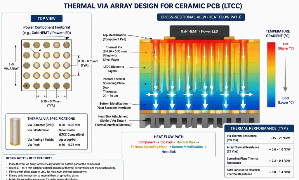
Via thermal resistance in ceramic substrates depends on via diameter, fill material, and aspect ratio. A 0.15mm diameter LTCC via filled with silver paste exhibits approximately 15-20°C/W thermal resistance over a 1mm depth, compared to 8-12°C/W for a 0.25mm via. Via arrays reduce effective thermal resistance through parallel heat paths; a 5×5 array of 0.15mm vias spaced 0.50mm apart provides approximately 0.6-0.8°C/W combined thermal resistance—sufficient for many moderate-power applications (2-5W dissipation per component).
For HTCC designs, via metallization with tungsten or molybdenum provides lower thermal conductivity than LTCC silver vias (tungsten: 174 W/mK vs silver: 429 W/mK). However, the substrate’s superior thermal conductivity compensates, and the overall thermal resistance from die to heat sink is typically better in HTCC AlN than LTCC, even with less conductive via metallization.
Conductor current capacity in ceramic PCBs must account for both electrical and thermal limits. A 0.20mm wide, 12 μm thick silver trace on LTCC can safely carry approximately 1.5A continuous current with 10°C temperature rise, assuming adequate thermal coupling to internal ground planes. For higher current requirements, increase trace width or use multiple parallel conductor layers connected by via stitching every 1-2mm. This multi-layer approach distributes current across several conductors, reducing I²R losses and improving thermal performance.
Thermal simulation is essential for ceramic PCB designs exceeding 5W total power dissipation. Standard PCB thermal analysis tools (Ansys Icepak, Mentor FloTHERM) support ceramic material libraries, but accurate simulation requires knowing the effective thermal conductivity of your specific LTCC or HTCC material, including the influence of via density and conductor planes. Many ceramic PCB manufacturers provide thermal modeling services using their validated material properties and process parameters.
Common thermal design errors in ceramic stackups include insufficient via density beneath power components, inadequate metal plane area for heat spreading, and poor thermal coupling between component pads and internal thermal planes. During design review, calculate the thermal resistance path from each significant heat source to the ultimate heat sink, and verify that junction temperature remains within component specifications across the full operating temperature range.
8. FAQ
What is the typical dielectric constant range for LTCC materials used in multi-layer stackups?
LTCC materials typically exhibit dielectric constants between 4.0 and 9.8 at RF frequencies, depending on the glass-ceramic composition. Low-Dk LTCC tapes (Dk ≈ 4.0-6.0) are preferred for millimeter-wave applications to minimize wavelength compression and reduce conductor loss, while higher-Dk materials (Dk ≈ 7.0-9.8) are used for size-constrained designs where compact layout is prioritized over absolute RF performance.
How does co-firing shrinkage affect dimensional accuracy in 8-layer LTCC designs?
LTCC tapes shrink 12-18% in the X-Y plane during co-firing, with slightly lower Z-axis shrinkage (10-15%). For 8-layer designs, cumulative tolerance stack-up can result in ±0.3-0.5mm positional error on 100mm × 100mm panels. Critical dimensions such as component mounting pads or RF cavity features may require post-fire laser machining or mechanical grinding to achieve ±0.1mm tolerance.
Can I mix LTCC and HTCC materials in the same stackup?
No, LTCC and HTCC cannot be directly combined in a single co-fired stackup due to incompatible firing temperatures (850°C vs 1600°C) and mismatched thermal expansion coefficients. However, hybrid modules can be assembled by separately manufacturing LTCC and HTCC substrates and then interconnecting them through wire bonding, flip-chip attachment, or interposer structures.
What via aspect ratio is achievable in 10-layer LTCC designs?
Ten-layer LTCC stackups can achieve via aspect ratios up to 10:1 or 12:1, depending on the tape thickness and via diameter. For example, a total stackup thickness of 1.2mm with 0.10mm diameter vias yields a 12:1 aspect ratio. However, manufacturing yield decreases significantly above 8:1, and via resistance increases due to incomplete paste filling in high-aspect-ratio features. For production designs, limiting aspect ratio to 8:1 is recommended.
How do I calculate trace width for 50-ohm impedance on AlN HTCC substrate?
For AlN HTCC with Dk ≈ 8.8 and 0.635mm dielectric thickness, a 50-ohm microstrip requires approximately 0.45mm trace width, assuming 8 μm tungsten conductor thickness. Use a field solver (Ansys HFSS, Keysight ADS) for accurate impedance calculation, as the simplified microstrip formula has limited accuracy for high-Dk ceramics. Verify impedance with TDR testing after fabrication, and specify ±10% impedance tolerance to account for manufacturing variation.
What is the minimum spacing between thermal vias in a via array under a power component?
Thermal via spacing in ceramic substrates typically ranges from 0.50mm to 1.00mm center-to-center, balancing thermal performance against routing congestion and mechanical strength. Closer spacing (<0.50mm) provides marginal thermal benefit but increases ceramic stress during co-firing and may cause delamination. For LTCC designs, 0.60-0.75mm spacing is optimal; for HTCC, 0.75-1.00mm is recommended due to larger minimum via diameter.
Does ceramic PCB stackup require ground stitching vias like FR4 designs?
Yes, ground stitching vias are essential in multi-layer ceramic PCBs for RF and high-speed digital designs. Stitch vias should be placed every λ/10 to λ/20 along ground plane boundaries to suppress cavity modes and reduce ground bounce. At 10 GHz on LTCC with Dk = 7.8, wavelength is approximately 10.7mm, requiring ground stitching every 0.5-1.0mm. Use 0.15mm diameter vias for stitching to minimize impact on routing density.
What surface finish options are available for ceramic PCB solderable pads?
LTCC silver or gold conductors typically receive nickel-gold (Ni/Au) plating for solderability: 3-5 μm electroless nickel followed by 0.05-0.10 μm immersion gold or flash gold. For HTCC tungsten/molybdenum conductors, a thicker electroplated nickel layer (5-10 μm) is required to provide a solderable surface, followed by gold finish. Some applications use solder paste screen-printing directly onto LTCC gold pads without additional plating, though this limits rework capability.
9. Conclusion and Design Recommendations
Optimizing multi-layer ceramic PCB stackups for 2-12 layer designs requires balancing material properties, electrical performance requirements, thermal management constraints, and manufacturing yield considerations. LTCC technology dominates RF and microwave applications where low dielectric loss and design flexibility are paramount, while HTCC—particularly aluminum nitride—is essential for high-power applications demanding superior thermal conductivity.
For designs up to 6 layers, focus on impedance control through accurate dielectric thickness specification and via geometry optimization. Beyond 6 layers, manufacturing tolerances and co-firing shrinkage become critical limiting factors, requiring increased via capture pads and more conservative trace spacing. Thermal management should be integrated into the stackup planning phase rather than addressed as an afterthought, particularly for designs exceeding 5W total power dissipation where via array placement and thermal plane configuration directly impact reliability.
If you’re developing a ceramic PCB design for RF, microwave, or high-power applications, our engineering team can provide stackup optimization recommendations based on your specific electrical and thermal requirements. Contact us for a free design review or download our ceramic PCB design guidelines for detailed layer planning worksheets and impedance calculation tools.