PCB Backdrilling: A Comprehensive Guide to Techniques, Benefits, and Applications
Introduction to PCB Backdrilling
Printed Circuit Board (PCB) backdrilling, also known as controlled depth drilling or counterboring, is an advanced manufacturing technique used to remove unused portions of through-hole vias in high-speed digital designs. This process has become increasingly critical in modern electronics as signal speeds continue to rise and signal integrity demands become more stringent.
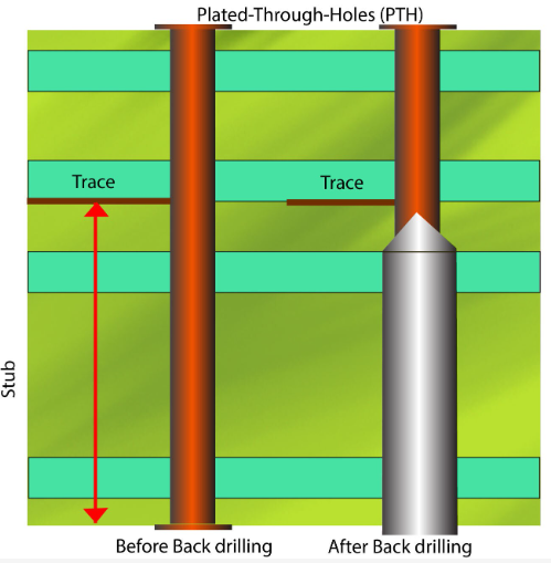
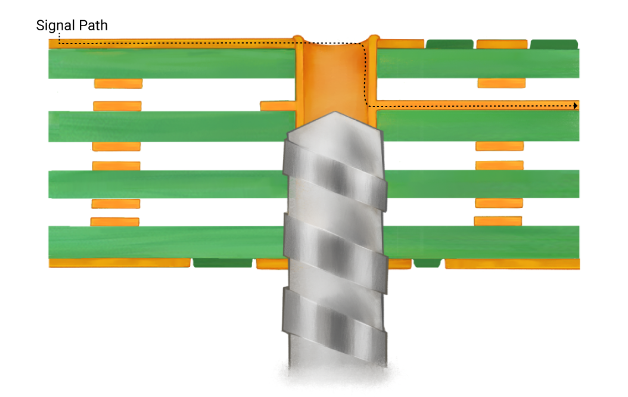
Backdrilling addresses one of the fundamental challenges in high-speed PCB design: the parasitic effects of via stubs. When a via connects only some of the layers in a multilayer PCB, the remaining unused portion acts as an antenna, reflecting signals and causing signal integrity issues. Backdrilling effectively eliminates these problematic via stubs, improving overall system performance.
The Physics Behind Backdrilling Necessity
To fully appreciate the importance of backdrilling, we must examine the electromagnetic phenomena that occur in high-speed PCBs:
- Signal Reflection Theory: When a high-frequency signal encounters an impedance discontinuity (like a via stub), a portion of the signal reflects back toward the source. These reflections cause signal distortion and timing errors.
- Stub Resonance Effects: Unused via portions act as resonant structures. At certain frequencies matching the stub’s electrical length, these resonances can completely disrupt signal transmission.
- Skin Effect Considerations: At high frequencies, current flows primarily on the conductor’s surface. Backdrilling removes unnecessary conductor material that could otherwise contribute to parasitic capacitance.
Mathematically, the resonant frequency of a via stub can be approximated by:
f_res = c / (4 × L_stub × √ε_r)
Where:
- c = speed of light
- L_stub = length of the via stub
- ε_r = dielectric constant of the PCB material
For a 10mm stub in FR-4 material (ε_r ≈ 4), resonance occurs around 3.75 GHz—squarely in the range of many modern digital signals.
Backdrilling Process: Step-by-Step
The backdrilling process involves precise mechanical operations:
- Initial Drilling: Standard through-holes are drilled completely through the PCB stackup.
- Plating: These holes are plated with copper as in conventional PCB manufacturing.
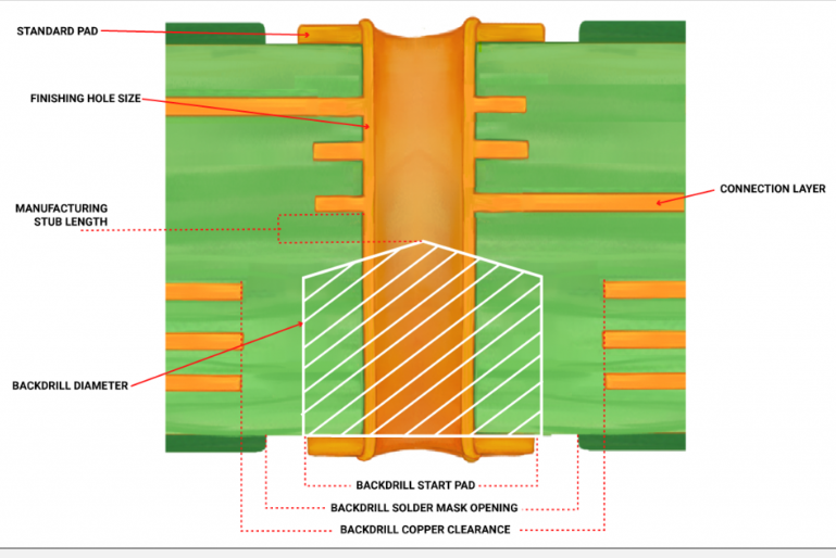
- Backdrill Tool Selection: Special drill bits with slightly larger diameters (typically 0.1-0.2mm larger than the original via) are chosen.
- Depth Control: Using precise depth-control mechanisms, the backdrill bit removes the copper plating from the unused portion of the via.
- Cleaning: The PCB undergoes thorough cleaning to remove any drilling debris.
Critical parameters in backdrilling:
- Diameter Tolerance: Typically ±0.05mm
- Depth Control Accuracy: ±0.075mm or better
- Positional Accuracy: ±0.05mm relative to original via
Technical Benefits of Backdrilling
- Improved Signal Integrity:
- Reduction in insertion loss (typically 1-3dB improvement at 10GHz)
- Decreased return loss (improvements of 5-10dB common)
- Elimination of resonant nulls in frequency response
- Enhanced Power Integrity:
- Reduced plane capacitance
- Lowered power supply noise
- EMI Reduction:
- Via stubs can radiate significantly (3-5dB reduction common with backdrilling)
- Better compliance with EMC standards
- Comparative Advantage Over Alternatives: Technique Cost Signal Integrity Manufacturability Backdrilling $$ Excellent Good Blind/Buried $$$$ Excellent Complex HDI Microvias $$$ Good Moderate Stub Routing $ Fair Easy
Design Considerations for Backdrilled PCBs
- Layer Stackup Planning:
- Signal layers should be grouped near the board surface
- Place critical signals to minimize required backdrill depth
- Via Placement Rules:
- Maintain ≥0.3mm clearance between backdrill and adjacent features
- Keep backdrilled vias ≥1.0mm from board edges
- Material Selection Factors:
- Glass transition temperature (Tg) affects drilling quality
- Resin content influences drill wear rates
- Low-ε_r materials show greater benefit from backdrilling
- Design Rule Checks:
- Implement specific DRC rules for backdrill overlap
- Verify annular ring requirements post-backdrilling
Manufacturing Challenges and Solutions
- Drill Breakage Prevention:
- Use carbide drills with specialized coatings
- Implement peck drilling cycles
- Maintain optimal spindle speeds (typically 80,000-120,000 RPM)
- Depth Control Techniques:
- Mechanical depth stops
- Laser measurement systems
- Vision-based depth verification
- Debris Management:
- High-pressure flush systems (≥30psi)
- Vacuum debris removal
- Ultrasonic cleaning post-process
- Quality Control Metrics:
- Cross-sectional analysis (sample rate: 1-5%)
- Time-domain reflectometry (TDR) testing
- High-frequency network analyzer measurements
Cost Analysis and Trade-offs
The economic considerations of backdrilling include:
- Direct Costs:
- Additional drilling step: $0.05-$0.20 per hole
- Increased board fabrication time: 10-30% longer
- Indirect Costs:
- Higher yield loss during learning curve
- Additional QA requirements
- Cost-Benefit Scenarios: Application Frequency Typical Benefit Cost Justified? Consumer 5G >24GHz Critical Yes Enterprise Switch 10-16GHz Significant Usually Automotive ADAS 6-10GHz Moderate Case-by-case Industrial Control <5GHz Minimal Rarely
Advanced Backdrilling Techniques
- Laser Backdrilling:
- Uses UV or CO₂ lasers for precision
- No mechanical drill wear
- Capable of smaller diameters (down to 50μm)
- Plasma Etching:
- Chemical removal of copper
- Excellent depth control
- Slow process speed
- Tapered Backdrills:
- Gradual impedance transition
- Reduced reflection at transitions
- Requires specialized drill bits
- Partial Backdrilling:
- Leaves short controlled stubs
- Useful for tuning applications
- Requires careful simulation
Industry Applications
- Telecommunications:
- 5G base stations (mmWave applications)
- Optical networking equipment (400G+ interfaces)
- High-Performance Computing:
- Server motherboards (PCIe 5.0/6.0)
- GPU accelerator cards
- Aerospace and Defense:
- Radar systems
- Satellite communications
- Electronic warfare systems
- Automotive:
- Autonomous vehicle sensors
- Vehicle-to-everything (V2X) systems
Future Trends in Backdrilling Technology
- Automation Integration:
- Machine learning for process optimization
- Automated optical inspection (AOI) for backdrill verification
- Materials Advancements:
- Low-loss dielectrics enabling higher frequencies
- Improved copper platings for smoother via walls
- Hybrid Techniques:
- Combined mechanical/laser approaches
- Additive manufacturing integration
- Design Tool Integration:
- 3D electromagnetic simulation of backdrilled vias
- Automated backdrill annotation in CAD tools
Conclusion
PCB backdrilling has evolved from a niche technique to a critical manufacturing process for high-speed digital designs. As data rates continue climbing toward 112Gbps and beyond, the importance of proper via management through backdrilling will only increase. While the process adds complexity and cost to PCB fabrication, the signal integrity benefits for high-frequency applications make it an essential tool in the electronics designer’s toolkit.
Successful implementation requires close collaboration between design engineers and manufacturing partners, with careful consideration of technical requirements versus economic constraints. With proper application, backdrilling can significantly improve system performance while maintaining manufacturability—a crucial balance in today’s competitive electronics marketplace.
The future of backdrilling will likely see increased automation, tighter integration with design tools, and the development of hybrid techniques combining the best aspects of mechanical and laser processes. As these advancements mature, backdrilling may become standard practice for an ever-wider range of PCB applications.