
PCB Design for Battery Management Systems (BMS)
Battery management system PCBs operate at the intersection of precision analog sensing and high-current power switching. A voltage measurement error of 10mV triggers false protection shutdowns; thermal hotspots at 85°C degrade balancing resistor tolerance by 15%. After designing BMS boards for EV and energy storage applications, success depends on proper current path design, isolation discipline, and thermal headroom.
This guide covers PCB layout decisions that determine whether your BMS achieves ±1mV cell voltage accuracy, whether balancing circuits survive 100,000 cycles, and whether your board meets automotive qualification.
High Current Path Design
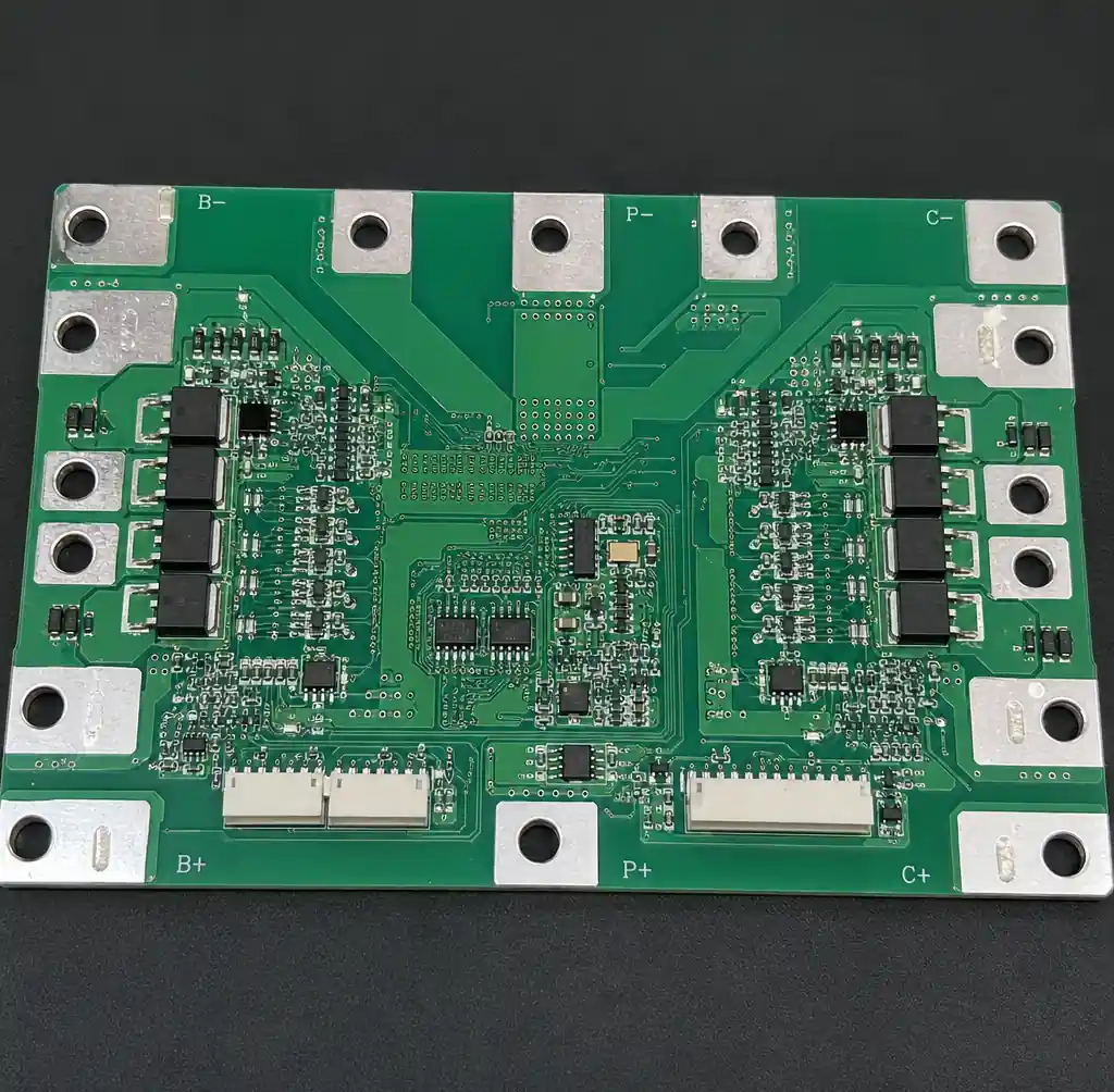
High current traces in BMS designs carry 50A to 300A+ for EV applications. For 100A continuous discharge on 2oz copper, you need approximately 400mil (10mm) trace width to limit temperature rise to 10°C. The challenge is the transition from board-mounted terminals to copper.
| Current Level | Copper Weight | Trace Width (2oz) | Trace Width (4oz) | Via Count (per amp) |
|---|---|---|---|---|
| 10-30A | 2oz | 120-200mil | 80-120mil | 2-3 vias |
| 30-100A | 3oz | 200-400mil | 150-250mil | 1-2 vias |
| 100-300A | 4oz+ | Bus bars | 300-500mil | Direct connection |
On power and energy BMS designs, 4oz copper for currents above 150A costs 15-20% more but delivers lower I²R losses and better thermal performance. Return paths must mirror power trace width—a 300mil power trace with 50mil return creates voltage ripple on sensing circuits.
Voltage Monitoring Circuit Layout
Cell voltage monitoring ICs like BQ76952 or LTC6813 require ±2mV accuracy across 2.5-4.5V range. Kelvin (4-wire) sensing separates high-current paths from measurement paths. Cell sense traces route on dedicated layers, isolated from switching noise.
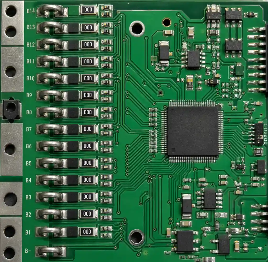
Each cell connection needs two paths: one carrying balancing current (up to 200mA), one carrying microamp-level sense current. Place a 0Ω resistor at each cell tap to create physical separation. High-current side connects to battery terminal; sense side connects to AFE IC input, eliminating voltage drop errors.
Sense trace impedance below 10Ω limits input bias errors. For 20cm routing, use minimum 10mil traces. Guard rings around high-voltage taps prevent leakage. On automotive PCB assemblies, add 0.5mm clearance between HV nets (>60V) and low-voltage logic.
Thermal Management for Balancing Circuits
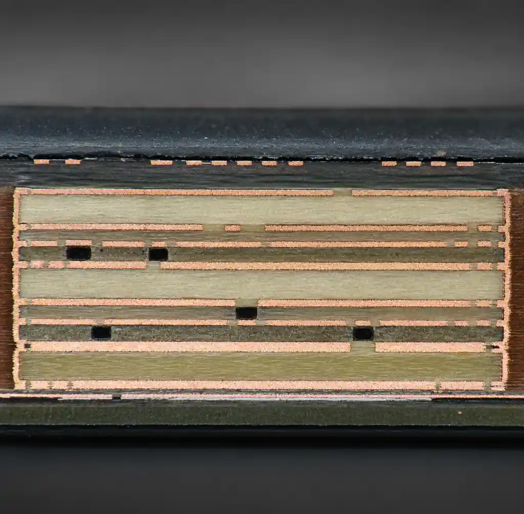
Passive cell balancing dissipates 0.5-2W per cell during equalization. For 16-cell packs, that’s 32W localized on your PCB. Poor thermal design causes board warping and accelerated aging.
| Balancing Current | Power per Cell | Thermal Via Density | Temperature Rise |
|---|---|---|---|
| 50mA | 0.2W | 4 vias/cm² | +15°C |
| 100mA | 0.4W | 8 vias/cm² | +25°C |
| 200mA | 0.8W | 16 vias/cm² | +40°C |
| 300mA | 1.2W | 24+ vias/cm² | +55°C |
Use 2512 or 2010 package resistors rated 1W for transient peaks. Each balancing resistor sits on copper pour connected to ground plane through thermal vias—minimum 0.3mm diameter, 0.6mm pitch. For 200mA balancing at 4V (0.8W), place 12-16 thermal vias under the component.
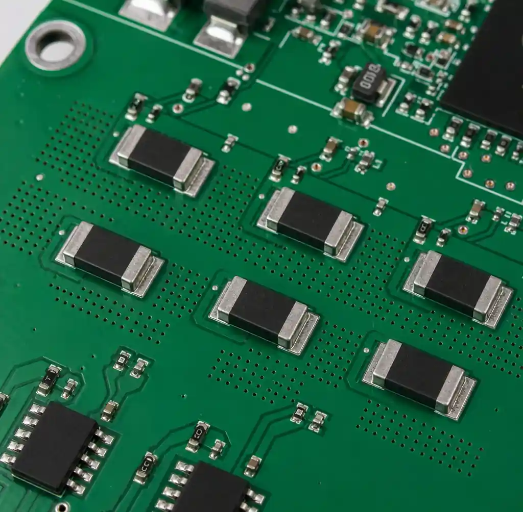
Maintain 15mm spacing between balancing resistors to prevent mutual heating. FR-4 has 0.3 W/m·K thermal conductivity; high-Tg FR-4 improves to 0.4 W/m·K.
Safety Isolation Standards
BMS designs require galvanic isolation between high-voltage battery pack (400-800V in EVs) and low-voltage control circuits (3.3-5V logic). IEC 60664-1 specifies minimum clearance of 3.2mm and creepage (surface distance) of 5.0mm for 400V working voltage. Design for 8mm creepage for reinforced isolation.
Digital isolators (ISO7741, ADuM1401) create communication barriers between AFE and microcontroller. Place isolation boundary 8mm from HV nets, route isolated power supplies separately, and use solid ground zones on each side. For automotive applications, ISO 26262 ASIL-D demands redundant isolation monitoring with leakage current detection.
Cell Balancing Circuit Optimization
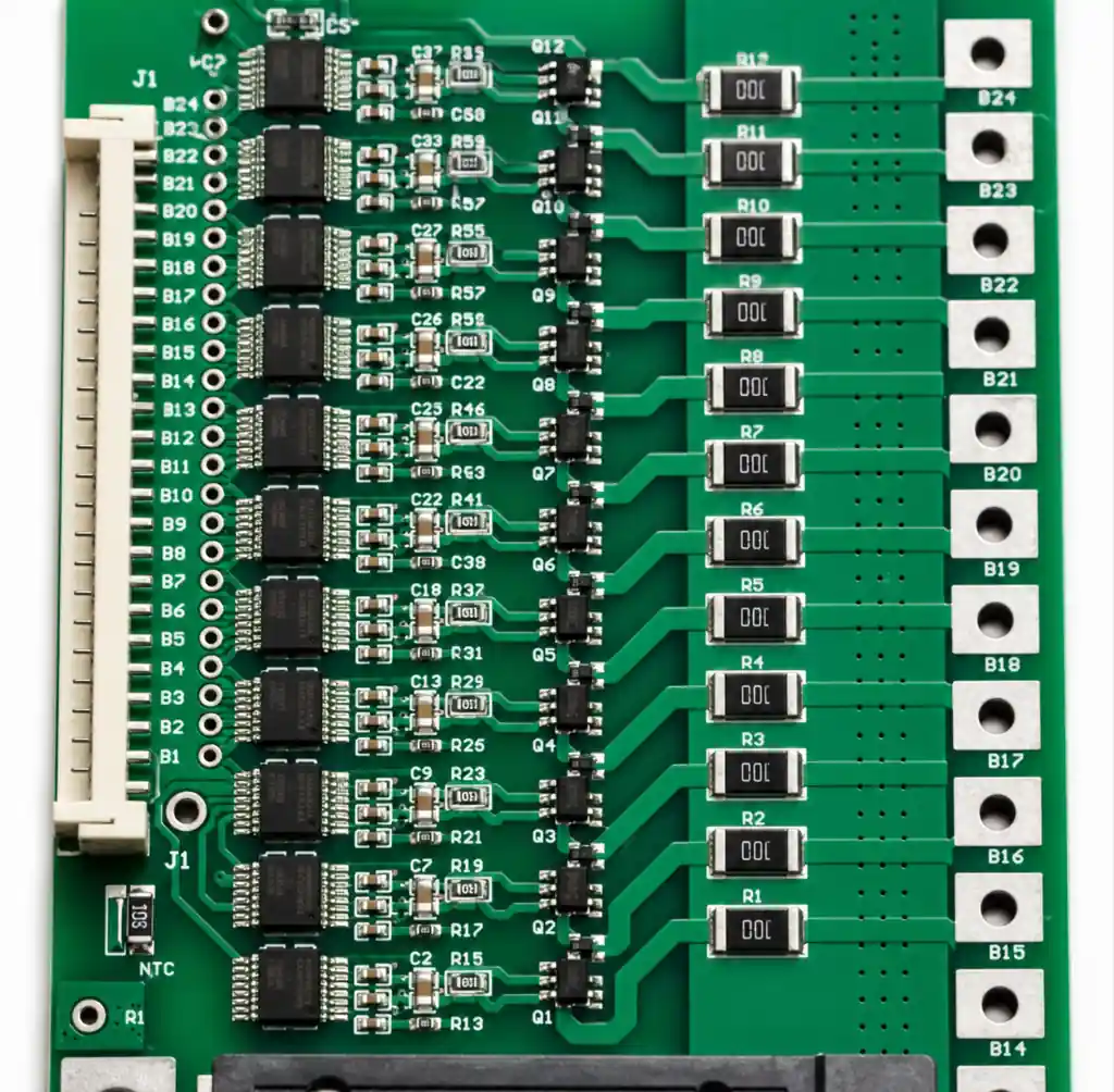
Each balancing FET (N-channel MOSFET, 30V 5A rated) switches the balancing resistor to ground. Keep gate driver trace length under 25mm to limit parasitic inductance. Place 10Ω gate series resistor close to FET. Resistor-to-FET connections use minimum 30mil traces for 200mA.
Active balancing (capacitive/inductive energy transfer) recovers 70-80% of imbalance energy but adds 40-60% cost. Passive balancing suffices for most applications with simpler PCB layout and proven reliability.
Automotive Component Selection
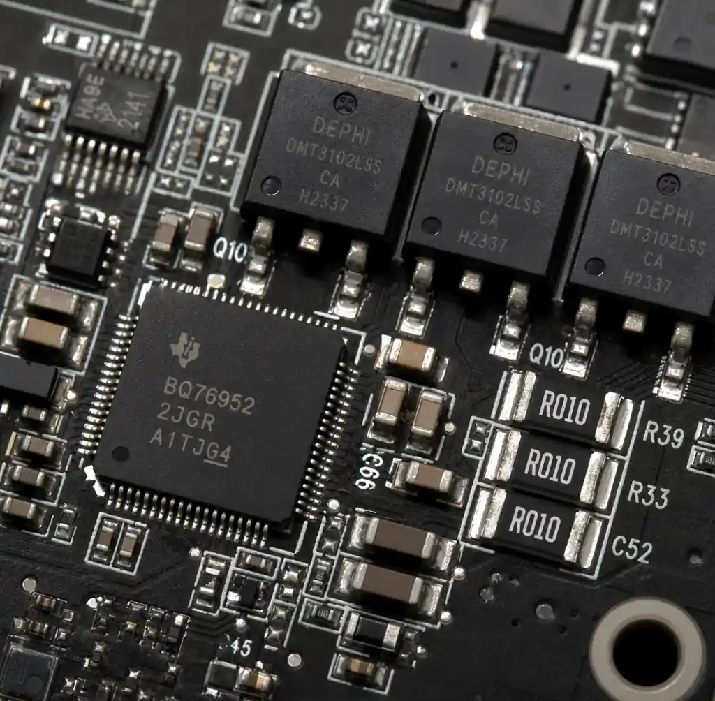
Components for automotive BMS survive -40°C to +125°C, pass AEC-Q100 stress testing, and support 15+ year life. Automotive-qualified parts prevent costly re-qualification.
| Component Type | Temperature Grade | AEC-Q100 Duration | FIT Rate |
|---|---|---|---|
| AFE IC | Grade 0 (-40 to +150°C) | 1000h HTOL | <100 |
| Balancing MOSFET | Grade 1 (-40 to +125°C) | 1000h HTOL | <50 |
| Ceramic Cap (X7R) | Grade 1 | 1000 cycles | <10 |
| Current Sense Resistor | Grade 1 | 1000h + 1000 cycles | <20 |
HTOL at 125°C for 1000 hours compresses 10 years of operation. Specify X7R or X5R ceramics; avoid Y5V types losing 70% capacitance at extremes. Use polymer electrolytics (125°C rated), not standard aluminum types.
Testing and Validation
Testing requires battery simulators, programmable loads, and thermal chambers. Standard sequence: flying probe testing (100% coverage), voltage measurement verification (±1mV across 2.0-4.5V), balancing current calibration (±5%), isolation resistance testing (>100MΩ HV-LV), thermal cycling (5 cycles -40°C to +85°C), and functional safety testing.
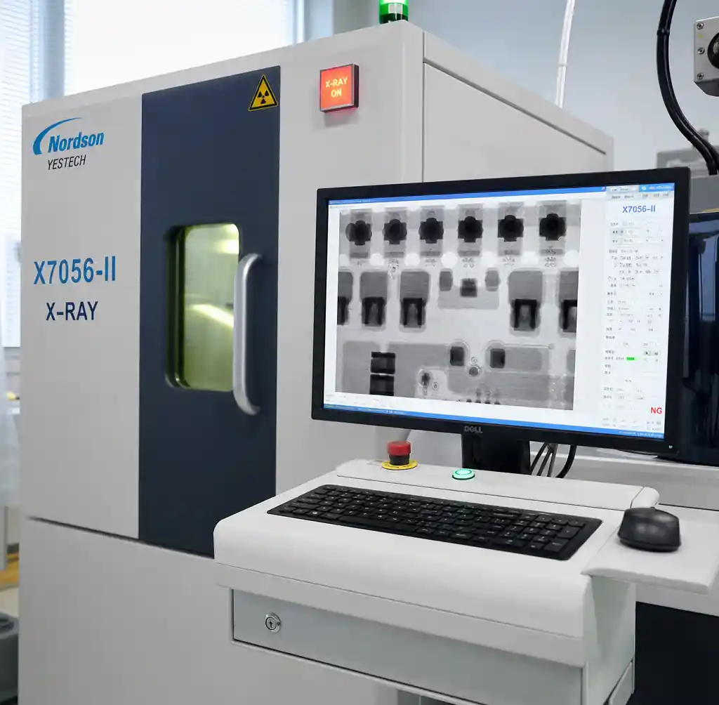
For automotive qualification, add 48-hour burn-in at 85°C, temperature shock, and vibration per AEC-Q100-011. X-ray inspection verifies solder joints—void content below 25% for power connections prevents electromigration failure.
Common Design Mistakes
Shared ground returns: Mixing sense and power ground injects noise. Separate AGND and PGND, connect at single star point near AFE IC.
Insufficient thermal relief: Standard thermal relief limits current. For terminals >10A, use solid connections or heavy thermal relief (8+ spokes, 0.5mm width).
Inadequate derating: Operating at 100% rating guarantees failures. Derate voltage to 80%, current to 75%, power to 60%.
Poor connector selection: Screw terminals introduce wear. Use bolted bus bar connections with Belleville washers.
Missing ESD protection: TVS diodes (SMAJ series) on each cell input within 5mm of connector protect against kilovolt strikes.
DFM Guidelines
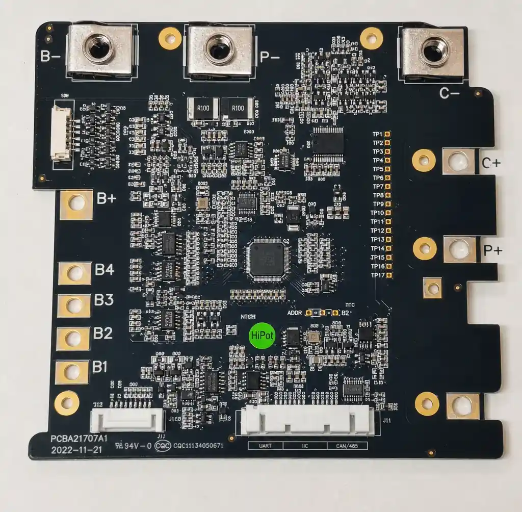
Start with reference designs from AFE IC manufacturers (TI, Analog Devices, Renesas) to save weeks. Key DFM practices: maintain 6mil minimum trace/space, limit PCB thickness to 2.0mm, use standard drill sizes (0.3-0.5mm), place fiducial marks for AOI, and add accessible test points. For volume >10,000 units/year, panelization reduces assembly cost by 30-40%.
FAQ
What copper weight for 100A discharge?
Use 3oz minimum for 100A continuous. Above 150A, transition to 4oz or bus bars. Calculate width for 10-15°C temperature rise.
How to achieve ±1mV voltage accuracy?
Implement Kelvin sensing with separate current/sense traces, dedicated analog ground, sense impedance <10Ω, short AFE-to-tap routing, and guard rings around HV nets.
Clearance between HV and logic circuits?
For 400V systems, maintain 8mm creepage and 3.2mm clearance per IEC 60664-1. Automotive requires 8-10mm reinforced isolation.
Thermal vias under balancing resistors?
For 200mA (0.8W), use 12-16 thermal vias (0.3mm diameter) per resistor. 16 vias/cm² density for components >0.5W.
AEC-Q100 temperature grade needed?
Grade 1 (-40 to +125°C) for most components. Grade 0 (-40 to +150°C) for AFE ICs near heat sources. All require 1000h HTOL and 1000 temperature cycles.
Active vs passive balancing?
Passive balancing suffices for most: lower cost, simpler layout, proven reliability. Active balancing justifies cost only for >100mV regular imbalance or thermal constraints.
Conclusion
BMS PCB design balances microamp-level sensing with hundred-amp power switching, precision analog near high-frequency digital, and cost within automotive qualification. Successful designs share disciplined current path planning, rigorous thermal analysis, and strict isolation enforcement.
Start with proven reference designs, validate against automotive standards early, and prototype with production copper weight and component grades. Test functional performance, thermal limits, measurement accuracy under load, and isolation across temperature. The BMS market evolves toward 800V, tighter integration, and wireless architectures, but PCB fundamentals—grounding, thermal management, isolation—remain constant.
Sources: