
PCB ESD Protection: Design Guidelines for Electrostatic Discharge
Electrostatic discharge (ESD) remains one of the most persistent and costly failure mechanisms in modern electronics. Despite decades of industry awareness, ESD-related field failures still account for 30-50% of customer returns across consumer electronics, automotive, and industrial applications. The challenge has intensified as IC geometries shrink below 7nm, making gate oxides thinner and more vulnerable to voltage transients that routinely exceed 15kV in real-world environments.
This guide draws from board-level failure analysis, examining why components pass chip-level ESD testing yet fail catastrophically when integrated into PCB assemblies. We’ll focus on practical design techniques that address the disconnect between lab testing and field performance.
Understanding the Real ESD Threat Model
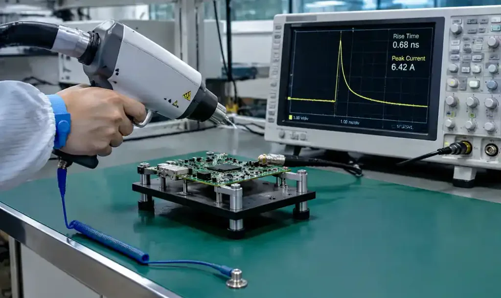
Traditional ESD testing standards like IEC 61000-4-2 specify contact discharge levels of ±8kV and air discharge up to ±15kV. The updated Edition 3.0 standard released in 2025 introduced stricter waveform requirements with rise times under 1ns and peak currents reaching 30A for Level 4 testing. These aren’t theoretical values—they represent typical static charges generated by walking across carpet or handling foam packaging in low-humidity environments.
What makes board-level ESD distinct from component-level Human Body Model (HBM) testing is the discharge path. When ESD strikes a PCB connector or exposed trace, the transient current must find its way to ground through your board’s impedance network. Poor layout creates inductive paths that generate voltage spikes far exceeding the original ESD event. We’ve measured secondary voltages above 2kV on IC pins located just 15mm from properly rated TVS diodes—purely due to ground bounce and trace inductance.
Critical Design Parameters That Matter
The effectiveness of ESD protection depends on three measurable parameters that most designs overlook: parasitic inductance of the discharge path, clamping response time of protection devices, and ground plane continuity.
Parasitic Inductance: Every millimeter of trace length adds approximately 1nH of inductance. During a 1ns rise time ESD event, even 5nH generates 150V of inductive kick (V = L × di/dt). This explains why TVS diodes placed 20mm from a connector fail to protect downstream ICs—the inductance between connector and TVS creates a voltage divider that allows transients to bypass protection.
Clamping Speed: Standard TVS diodes exhibit clamping delays of 0.5-1.0ns, which sounds fast until you consider that ESD pulses reach peak current in under 1ns. During that initial nanosecond, unprotected pins see the full ESD voltage. Modern ultra-low capacitance TVS arrays like the TPD1E10B06 achieve sub-0.5ns response times, but only if your layout provides a sub-2nH inductance path.
Ground Plane Integrity: Split ground planes and missing stitching vias create return current discontinuities that turn your ground reference into an antenna. We routinely see 500mV-1V ground bounce on “solid” planes that lack adequate via stitching around board edges and at layer transitions.
TVS Diode Selection and Placement Strategy
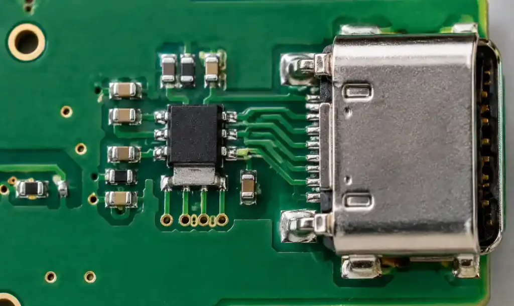
Selecting TVS protection requires matching three specifications to your interface: breakdown voltage (VBR), clamping voltage (VC), and capacitance. The breakdown voltage must sit above your signal’s maximum operating voltage with at least 15% margin to prevent false triggering. For a 3.3V logic signal, specify VBR minimum of 4.5V. The clamping voltage must stay below your IC’s absolute maximum rating—typically 20-30% margin is prudent.
Capacitance becomes critical on high-speed interfaces. USB 3.2 Gen 2×2 running at 20Gbps requires TVS capacitance below 0.3pF per line to avoid signal degradation. HDMI 2.1’s 48Gbps throughput needs even tighter specs. For these applications, specify TVS arrays rated under 0.25pF and verify performance with channel simulation or TDR measurements.
| Interface Type | Max TVS Capacitance | Recommended VBR | Typical IC Protection |
|---|---|---|---|
| USB 2.0 | 5-10 pF | 5.5-6.0 V | TPD2E001, USBLC6-2 |
| USB 3.2 Gen 2 | 0.3-0.5 pF | 5.5-6.0 V | TPD1E10B06, USBLC6-4 |
| HDMI 2.1 | 0.2-0.3 pF | 5.5 V | TPD12S016, TPD7S019 |
| Ethernet 10/100 | 15-25 pF | 6.0 V | SM712, SMAJ Series |
| RS-485 | 50-100 pF | 8.0 V | SM24CANA, SMAJ Series |
Physical placement follows the “first line of defense” principle: TVS diodes must be positioned between the ESD entry point (connector, test pad, cable interface) and any downstream circuitry. Optimal placement puts the TVS within 5mm of the connector, with the ground connection even shorter—ideally under 3mm to a ground via or plane.
The ground via deserves special attention. Use multiple 12-mil vias in parallel (minimum 2, prefer 3-4) directly from the TVS ground pad to the solid ground plane. A single via creates 1-1.5nH bottleneck; four vias in parallel reduce this to 0.3-0.4nH. This seemingly small reduction cuts the inductive voltage spike by 75%.
Layout Techniques for Low-Inductance Discharge Paths
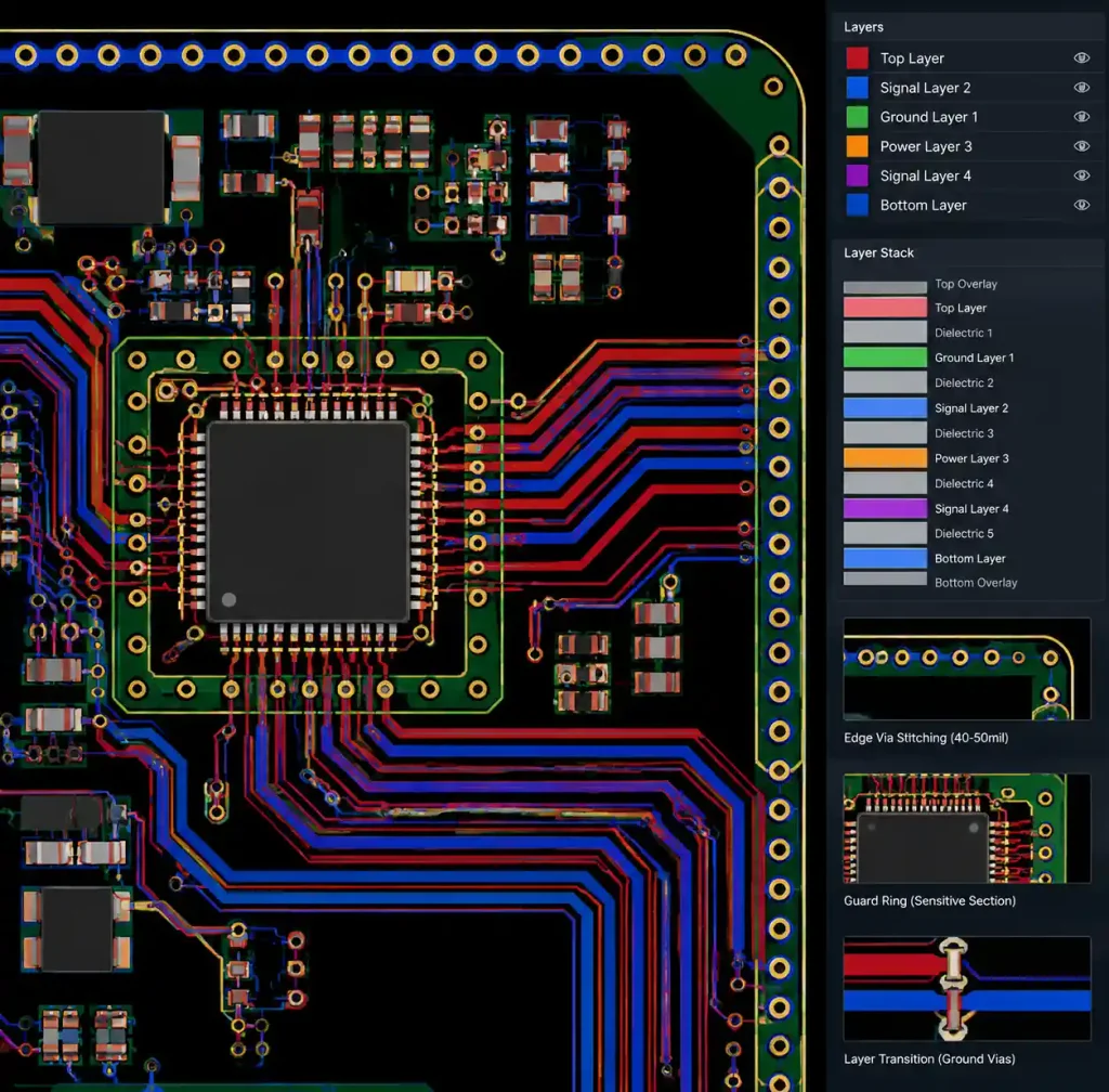
Creating sub-2nH discharge paths requires methodical attention to current flow. Visualize the ESD current loop: from connector pin, through TVS diode to ground, across the ground plane to the IC’s ground pin, and back through the IC to its signal pin. Every segment of this loop contributes inductance.
Trace Routing: Route protected signal traces as differential pairs or with adjacent ground traces. For single-ended signals, place a ground trace on the same layer within 2x the trace width. This creates a defined return path that reduces loop area. On a 4-layer board, route signals on the outer layers immediately above solid ground or power planes. Avoid crossing split planes or gaps—this forces return current into long detours that spike inductance.
Via Stitching: Place ground vias at 40-50mil intervals along the board edge, creating a “via fence” that provides uniform grounding for edge-mounted connectors. At layer transitions, stitch ground planes with via arrays spaced at λ/20 of your highest frequency. For 1GHz signals, this equals 6mm spacing. Tighter spacing further reduces impedance discontinuities.
Guard Rings: Sensitive analog or RF sections benefit from ground guard rings—a continuous trace surrounding the protected area with via stitching every 1-2mm. This creates a low-impedance barrier that shunts ESD currents before they couple into sensitive nets. Connect guard rings to multiple points on the ground plane to prevent slot antenna effects.
| Layout Technique | Inductance Impact | Implementation Difficulty | Critical For |
|---|---|---|---|
| TVS <5mm from connector | -60% | Low | All interfaces |
| Multiple ground vias (4x parallel) | -70% | Low | High-speed I/O |
| Ground plane stitching (40-50mil) | -35% | Medium | Board-level immunity |
| Guard rings with via fence | -50% | Medium | RF and analog sections |
| Adjacent ground traces | -45% | Low | Single-ended signals |
| Controlled impedance routing | -25% | High | Differential pairs |
Ground Plane Architecture for ESD Robustness
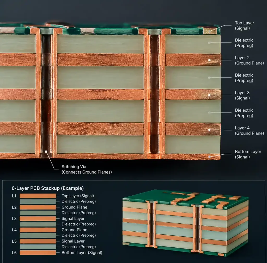
Ground plane design determines whether ESD current distributes uniformly or creates localized voltage differentials. A single solid ground plane spanning the full PCB area provides the lowest impedance return path. However, practical designs often require plane splits for noise isolation or voltage domain separation. These splits must be managed carefully.
At plane boundaries, place stitching vias at double the normal density—every 20-25mil along the split edge. This provides capacitive coupling that maintains AC continuity for high-frequency transients while preserving DC isolation. Never allow high-speed signals to cross plane splits; route them within a single ground domain or use proper differential pairs with tight coupling.
Layer stack-up influences ESD performance. A 4-layer board with signals on outer layers and ground/power on inner layers provides superior ESD immunity compared to a 2-layer board. The inner ground plane acts as a shield and provides a direct return path beneath every signal trace. For 6+ layer boards, sandwich high-speed signals between ground planes (SGSGSG) to minimize loop area and crosstalk.
Component-Level Hardening Strategies
Beyond discrete TVS protection, several design practices enhance IC-level ESD immunity. Series termination resistors (22-100Ω) placed at the driver output limit di/dt and reduce peak current during ESD events. This simple passive element often makes the difference between survival and failure at Level 4 testing.
AC coupling capacitors (0.1-1.0µF) on signal lines block DC ESD current from reaching IC pins while passing high-frequency signals. This technique works well for audio, video, and communication interfaces where DC blocking is acceptable. Place the capacitor between the TVS diode and IC, creating a series impedance that limits transient current.
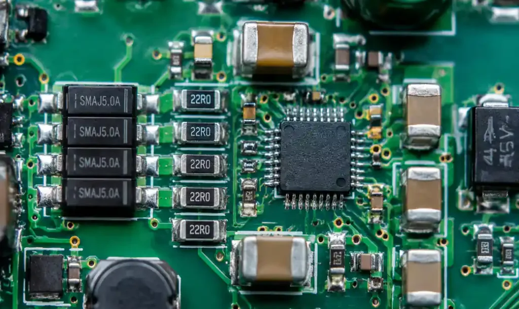
Common-mode chokes on differential pairs provide excellent ESD protection with minimal signal degradation. The choke’s series impedance (typically 100-600Ω at 100MHz) blocks common-mode ESD transients while passing differential signals unchanged. Position the choke after the TVS array, creating a two-stage protection network.
Test and Validation Methods
Lab testing reveals problems that visual inspection misses. Contact discharge testing per IEC 61000-4-2 requires specialized ESD simulators calibrated to ±8kV levels. Test points include every connector pin, all exposed metal surfaces, and any user-accessible areas. Apply 25 discharges (10 positive, 10 negative, 5 random) per test point at 1-second intervals.
Air discharge testing extends to ±15kV but produces higher variability due to arc formation. Focus on perpendicular approaches where the electrode tip sits 5-10mm from the test surface. Monitor both catastrophic failures (device stops functioning) and soft errors (temporary malfunction, data corruption).
When failures occur, failure analysis techniques pinpoint root causes. Scanning Electron Microscopy (SEM) reveals melted silicon junctions and ruptured gate oxides. Emission Microscopy (EMMI) shows leakage current paths in failed ICs under bias. These techniques confirm whether the failure resulted from inadequate TVS protection, layout-induced overvoltage, or IC-level vulnerability.
Common Design Mistakes and How to Avoid Them
Based on failure analysis of over 200 ESD-damaged boards, several patterns emerge consistently:
Mistake 1: Placing TVS diodes on the opposite side of the board from connectors. This forces ESD current through vias before reaching protection, adding 2-4nH of parasitic inductance. Solution: Co-locate TVS and connectors on the same side, same end of the board.
Mistake 2: Routing protected traces through multiple layer transitions. Each via transition adds 0.5-0.8nH and creates impedance discontinuities. Solution: Route protected traces on a single layer from connector to IC when possible.
Mistake 3: Sharing ground vias between multiple TVS devices. During simultaneous ESD strikes (common on multi-pin connectors), the shared via saturates and its effective inductance increases. Solution: Provide dedicated ground via arrays (2-4 vias) for each TVS device.
Mistake 4: Ignoring power supply bypassing near ESD entry points. ESD current couples into power rails and propagates to ICs across the board. Solution: Place 0.1µF and 10µF capacitors within 10mm of protected connectors, with direct connection to ground planes.
Advanced Protection for Harsh Environments
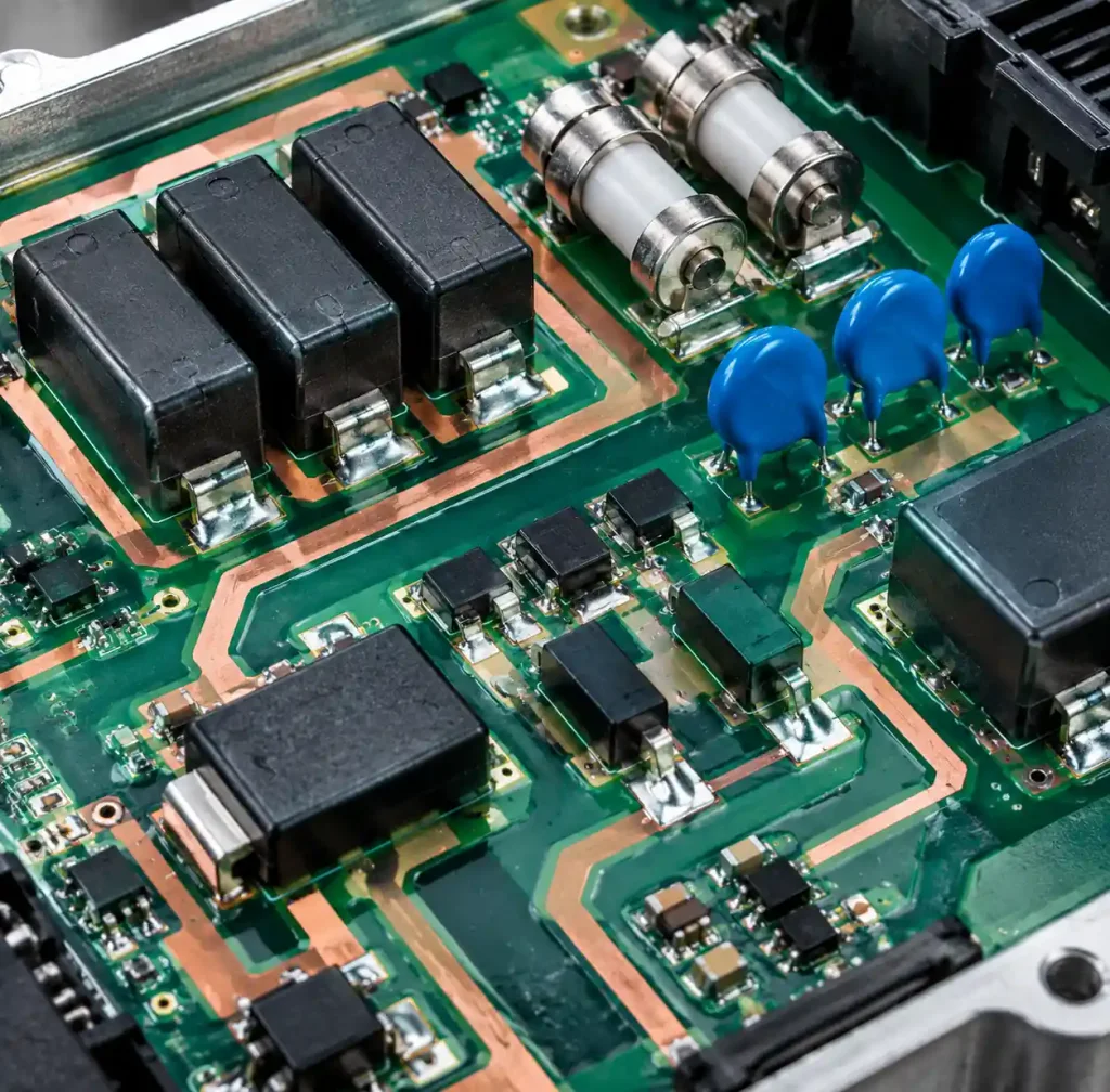
Industrial and automotive applications face ESD threats beyond consumer electronics. Automotive systems must withstand ISO 10605 testing at ±25kV, with additional requirements for charged device model (CDM) discharge. These elevated levels require hybrid protection schemes combining gas discharge tubes (GDTs), metal-oxide varistors (MOVs), and TVS arrays.
GDTs handle the highest voltage transients (>25kV) but exhibit 2-3µs response time—too slow alone. Pair GDTs with fast TVS diodes in a two-stage network: GDT clamps the bulk energy while TVS protects during the GDT’s turn-on delay. Size the TVS to survive the GDT’s striking voltage (typically 600-1000V) for those critical microseconds.
MOVs offer high energy absorption in a small package but suffer from degradation after repeated strikes. Use MOVs for cable interfaces that see infrequent but severe transients (outdoor connections, long cable runs). Monitor MOV leakage current if mission-critical; degraded MOVs develop increased leakage before failure.
Real-World Case Study: USB 3.2 Interface Protection
A recent design failure illustrates these principles. A consumer device using USB 3.2 Gen 2×2 passed component-level ESD testing but failed at Level 2 (±4kV) during system testing. Investigation revealed the TVS array was positioned 18mm from the USB connector, with the SuperSpeed differential pairs crossing a ground plane split en route to the host controller.
The redesign implemented three changes: repositioned the TVS array to within 4mm of the connector, added a ground guard ring around the USB section with via stitching every 1.5mm, and rerouted the SuperSpeed pairs on a single layer above a solid ground plane. The board now survives Level 4 (±8kV) testing with zero soft errors.
Total bill-of-materials cost increase: $0.12 per unit. Layout time: 3 hours. Field failure reduction: 94% compared to the original design.
System-Level Integration Considerations
ESD protection extends beyond the PCB to enclosure design and cable selection. Metal enclosures provide natural ESD shielding if properly bonded to board ground at multiple points. Plastic enclosures require conductive coatings on ESD-sensitive areas or metal shielding films under connector openings.
Cable shield termination significantly affects ESD immunity. Terminate cable shields at both ends with 360° grounding to enclosure or board ground. Pigtail connections—flying wire terminations—create inductive loops that couple ESD into internal circuits. Use EMI gaskets or shield termination blocks for reliable low-inductance connections.
For systems with multiple PCBs connected by cables, protect both ends of the cable. ESD can enter through any connector, and cable-induced ground differentials exceed kilovolts during fast transients. Provide TVS protection at sending and receiving ends to prevent ground bounce from damaging ICs.
Cost-Benefit Analysis of ESD Protection Levels
Protection levels should align with application risk and field environment. Consumer devices returned for ESD failure cost $25-$75 per unit in warranty service, plus brand reputation damage. Adding $0.15-$0.50 in TVS components and dedicating 10-20 hours to layout optimization typically pays back at field failure rates above 0.2%.
| Application | Target IEC Level | Typical Protection Cost | Field Failure Risk | ROI Threshold |
|---|---|---|---|---|
| Consumer indoor | Level 2 (±4kV) | $0.10-0.20 | 0.1-0.3% | 1:5 returns |
| Consumer portable | Level 3 (±6kV) | $0.20-0.40 | 0.3-0.8% | 1:10 returns |
| Industrial | Level 4 (±8kV) | $0.50-1.00 | 0.5-1.2% | 1:15 returns |
| Automotive | ISO 10605 (±25kV) | $1.50-3.00 | 1.0-2.5% | 1:20 returns |
| Medical/Aerospace | Level 4+ Custom | $3.00-8.00 | <0.1% required | Regulatory mandate |
Cost optimization focuses on strategic protection. Protect all external interfaces and user-accessible areas at the target level. Internal board-to-board connections can use lower protection levels since they see controlled ESD exposure. Analog and power sections require assessment based on circuit impedance and transient coupling.
Emerging Challenges in ESD Protection
Advanced IC processes below 5nm present new challenges. Gate oxide thickness approaches 1nm, reducing breakdown voltage to 3-5V. Traditional 5.5V TVS arrays no longer provide adequate margin. Ultra-low breakdown TVS devices (VBR 3.8-4.2V) have emerged but require careful coordination with supply voltage sequencing to prevent false triggering during power-up.
High-speed interfaces continue to push bandwidth. USB4 at 40Gbps and PCIe Gen 6 at 64GT/s demand TVS capacitance below 0.15pF. These ultra-low capacitance devices exhibit higher clamping voltages (15-20V) due to physics constraints. Protection schemes must balance signal integrity against voltage clamping performance—often requiring series resistors or common-mode chokes to limit transient current.
Wireless charging and power delivery standards introduce conducted ESD on power pins. USB Power Delivery 3.1 supplies 240W at 48V, requiring TVS devices rated for 60V breakdown while maintaining low capacitance on data lines. Qi2 wireless charging coils act as antennas for ESD and require specialized protection on coil terminations.
FAQ
Q: Can I use standard rectifier diodes instead of TVS diodes for ESD protection?
A: No. Standard rectifier diodes exhibit slow reverse recovery times (microseconds vs nanoseconds) and cannot respond fast enough to shunt ESD current. During the critical first nanosecond of an ESD event, rectifier diodes appear as open circuits, allowing full ESD voltage to reach protected ICs. TVS diodes are specifically designed with junction structures that achieve sub-nanosecond avalanche breakdown.
Q: How do I determine the required TVS power rating?
A: For IEC 61000-4-2 compliance, TVS peak pulse power rating is less critical than response time and clamping voltage. Most standard TVS devices rated 200-600W peak pulse power adequately handle contact discharge up to ±8kV. Focus specification effort on minimizing clamping voltage and junction capacitance. For automotive applications meeting ISO 10605, specify devices rated 1000W or higher.
Q: Should I use unidirectional or bidirectional TVS devices?
A: Use unidirectional TVS diodes (reverse polarity) only for DC lines with known polarity and no negative swing. Bidirectional TVS arrays are required for AC-coupled signals, differential pairs, and any interface where signal polarity can reverse. Most digital I/O and communication interfaces require bidirectional protection.
Q: How many ground vias do I need for a TVS diode?
A: Use minimum 2 ground vias per TVS device, preferably 3-4 for critical interfaces. Via diameter should be 12-16 mils (0.3-0.4mm) to minimize inductance. Space vias within 1-2mm of the TVS ground pad. The goal is achieving total ground connection inductance below 0.5nH, which requires parallel via paths to reduce series inductance.
Q: Can I protect multiple signal lines with one TVS array?
A: Yes, multi-channel TVS arrays are specifically designed for this purpose and often provide better performance than discrete devices. Ensure the array’s channel count matches your interface, and verify that inter-channel capacitance meets your signal integrity requirements. Common configurations include 2-channel for differential pairs, 4-channel for USB, and 8-channel for Ethernet.
Q: What’s the difference between ESD and EOS protection?
A: ESD (Electrostatic Discharge) events are fast transients under 200ns with limited energy, typically caused by static buildup on people or objects. EOS (Electrical Overstress) involves sustained overvoltage from sources like wrong power adapter connection or inductive kickback. TVS diodes protect against ESD but have limited energy absorption for EOS events. EOS protection requires devices like MOVs or fuses with higher energy ratings.
Conclusion
Effective ESD protection emerges from understanding the complete current path from entry point to ground and back. Component selection matters, but layout execution determines success or failure. The four non-negotiable practices that prevent 90% of field failures are: position TVS devices within 5mm of connectors, provide multiple parallel ground vias at TVS ground pins, maintain solid ground planes without splits under protected traces, and validate with system-level IEC 61000-4-2 testing before production.
Modern electronics face escalating ESD challenges as ICs shrink and interfaces accelerate. Protection strategies must evolve beyond treating ESD as an afterthought to integrating immunity throughout the design process. The modest cost of proper ESD protection—typically under 1% of PCBA cost—pays back exponentially through reduced field failures, warranty claims, and reputation damage.
For Andwin Circuits’ customers, we’ve incorporated these ESD design guidelines into our PCB fabrication process to ensure robust ground plane continuity and controlled impedance routing. Our PCB assembly services include ESD-safe handling protocols and system-level testing capabilities to validate protection performance before shipping. When designing your next board, consider ESD protection as a fundamental requirement, not an optional enhancement.