
PCB Teardrops: When to Use and How They Improve Reliability
PCB teardrops are teardrop-shaped copper fills added at the junction between traces and pads or vias. Industry data shows that drilling misalignment causes up to 15% of annular ring failures in high-volume production. These failures lead to open circuits and field returns that could be prevented with proper teardrop implementation.
If you design PCBs for automotive, medical, aerospace, or any application where reliability is non-negotiable, you need to understand when teardrops add value versus when they create unnecessary routing constraints. This guide provides decision frameworks based on IPC standards and real manufacturing data from Class 2 and Class 3 production environments.
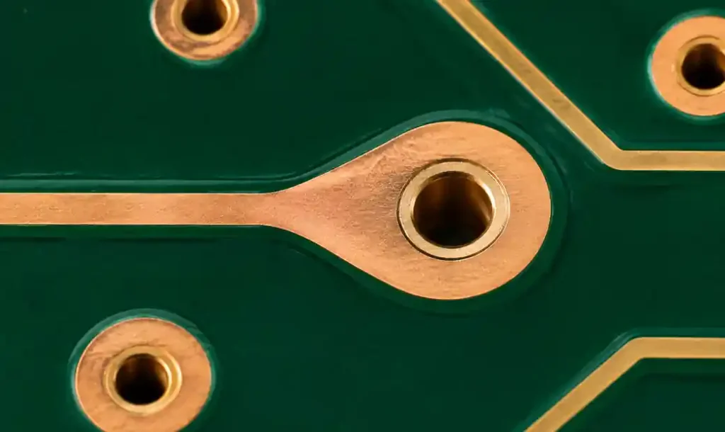
What Are PCB Teardrops and Why Do They Matter?
PCB teardrops are additional copper shapes that create a gradual transition from trace to pad or via, replacing the sharp 90-degree junction with a smooth curved fillet. The teardrop extends from the trace edge to the pad circumference, typically covering 30-60% of the pad area depending on design rules.
These features serve two critical functions: mechanical stress relief and annular ring protection. When drilling operations shift by 0.05-0.1mm from nominal position, a standard trace-to-via connection may lose contact entirely if the annular ring is minimal. The teardrop expands the effective connection zone, maintaining electrical continuity even with manufacturing tolerances.
Teardrops become essential in high-reliability applications where board flexing, thermal cycling, and vibration create repeated stress at solder joints. IPC-6012 Class 3 designs for military and medical applications often mandate teardrops on all via connections. However, for consumer electronics with 2-3 year lifespans, the routing complexity may outweigh the reliability gain.
When to Use Teardrops in PCB Design
High-vibration environments demand teardrops on every via and pad connection. Automotive underhood electronics, industrial control systems near motors, and transportation equipment experience continuous mechanical stress. Studies show teardropped connections survive 3-5x more thermal cycles before solder joint fatigue compared to sharp-angle junctions.
Class 3 PCB manufacturing requires teardrops per IPC-6012E specifications for life-critical applications. Medical implantable devices, aerospace avionics, and military equipment fall into this category where a single failure could cause loss of life. Fabricators audit designs for teardrop compliance before production begins.

Fine-pitch BGAs with annular rings below 0.15mm benefit significantly from teardrops. When pad diameter approaches via diameter, manufacturing tolerances consume most of the connection area. A 0.2mm via with 0.4mm pad leaves only 0.1mm annular ring on each side—any drilling offset exceeding 0.05mm risks breakout. Teardrops extend this margin by 40-60%.
| Application | Teardrop Requirement | Reason | IPC Class |
|---|---|---|---|
| Automotive electronics | Mandatory | Vibration, thermal cycling | Class 3 |
| Medical devices | Mandatory | Reliability, IPC-6012 Class 3 | Class 3 |
| Consumer IoT | Optional | Cost vs marginal benefit | Class 2 |
| Aerospace avionics | Mandatory | Mission-critical reliability | Class 3 |
| Industrial control | Recommended | Harsh environment operation | Class 2/3 |
Mechanical Stress Relief and Fatigue Resistance
Sharp-angle trace-to-pad transitions concentrate mechanical stress in a single point. When boards flex during handling or thermal expansion creates differential movement between copper layers, this stress point becomes a crack initiation site. Copper fatigue progresses through repeated load cycles until trace separation occurs.
Teardrops distribute stress across a curved transition zone spanning 0.3-0.8mm depending on trace width. The gradual geometry change reduces peak stress by 40-60% compared to right-angle connections. Finite element analysis shows stress concentration factors drop from 3.5× for sharp corners to 1.8× with properly sized teardrops.
Solder joint reliability improves because the copper pad provides a larger mechanical anchor. During reflow, solder wets the entire teardrop surface, creating a stronger metallurgical bond. This becomes critical for large components like connectors and transformers where inertial forces during board handling can crack inadequate joints.
Flexible and rigid-flex PCBs require teardrops in all dynamic flex zones. When copper bends repeatedly, standard trace-to-pad connections fail within 1,000-10,000 cycles. Teardropped connections tested per IPC-6013 survive 100,000+ flex cycles before degradation. The curved geometry accommodates bending without creating stress risers that propagate cracks.
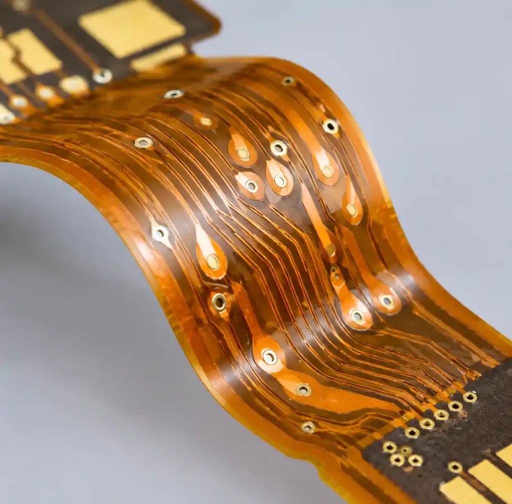
Annular Ring Protection During Manufacturing
PCB drilling accuracy ranges from ±0.05mm for precision shops to ±0.1mm for standard production. When a 0.3mm via with 0.5mm pad experiences 0.08mm offset, the minimum annular ring drops to 0.02mm on one side—below IPC-A-600 Class 2 requirements of 0.05mm. Teardrops compensate by extending copper coverage 0.2-0.3mm beyond the nominal pad edge.
Registration errors between layers compound drilling tolerance. Internal vias connecting layer 2 to layer 5 in an 8-layer stack must align with outer layer pads. Layer-to-layer misregistration of 0.075mm plus drilling offset of 0.075mm creates 0.15mm total error. Without teardrops, this exceeds the entire annular ring on a 0.4mm pad.
Post-drilling processes like plating and etching further reduce effective annular ring. Copper thickness variations of ±1oz (±35µm) mean the finished pad may be 0.07mm smaller than designed. Teardrops maintain electrical connection even when multiple manufacturing variations align in worst-case combinations.
Automated optical inspection systems flag marginal annular rings during electrical test. Boards with <0.05mm remaining copper around drilled holes fail IPC Class 2 requirements and face rework or scrap. Adding teardrops reduces annular ring failures by 60-80% in high-volume production, directly improving yield and reducing manufacturing cost.
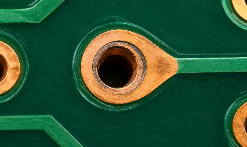
Teardrop Design Rules and Geometry
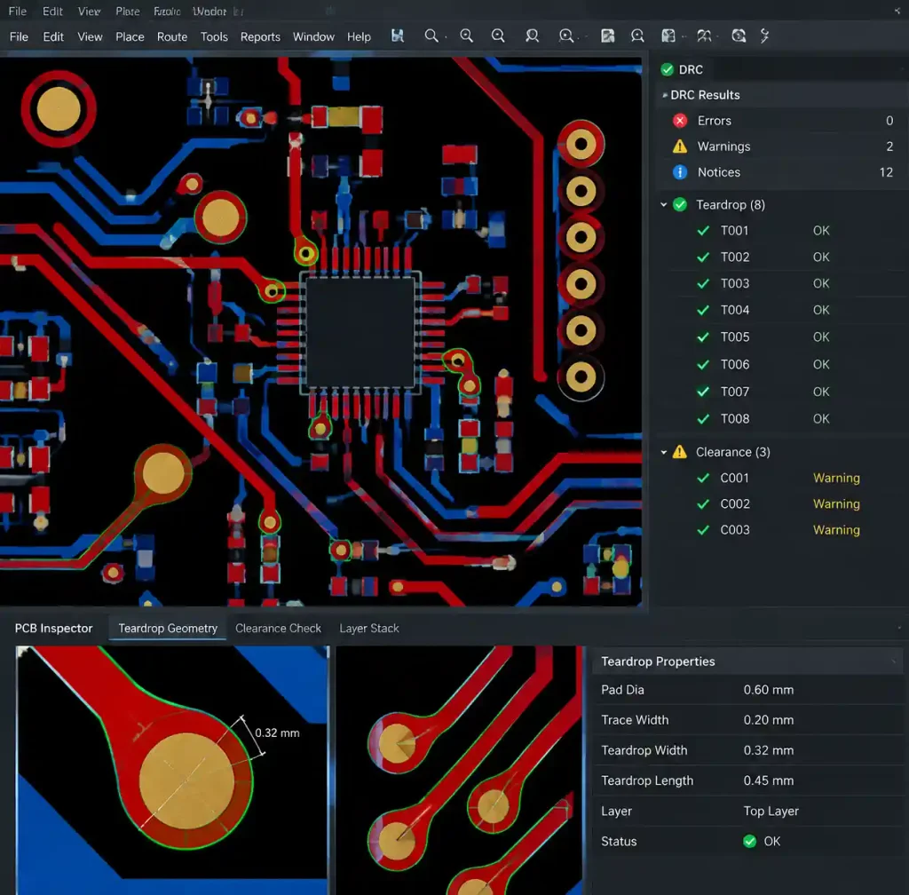
Standard teardrop geometry extends 2-3× the trace width along the trace direction and smoothly curves to meet the pad tangentially. For a 0.15mm trace connecting to a 0.6mm via pad, the teardrop length spans 0.3-0.45mm with maximum width matching the pad diameter. The curved profile prevents sharp angles that reintroduce stress concentration.
IPC-2221 recommends minimum fillet radius equal to trace width for stress relief effectiveness. Sharper curves save routing space but sacrifice mechanical benefits. Most EDA tools generate teardrops with 45-60 degree entry angles and Bézier curve profiles that balance space efficiency with stress distribution.
| Teardrop Parameter | Minimum | Recommended | Maximum |
|---|---|---|---|
| Length (trace width multiple) | 2× | 3× | 5× |
| Entry angle | 30° | 45-60° | 90° |
| Fillet radius | 1× trace width | 1.5× trace width | 2× trace width |
| Pad coverage | 20% | 40-50% | 70% |
Differential pair routing requires matched teardrops to maintain impedance consistency. Asymmetric teardrop geometry on coupled lines creates impedance discontinuities exceeding 5-8 ohms, causing reflections in high-speed signals above 1 Gbps. Symmetric teardrops on both traces preserve the 100-ohm differential impedance with <2 ohm variation.
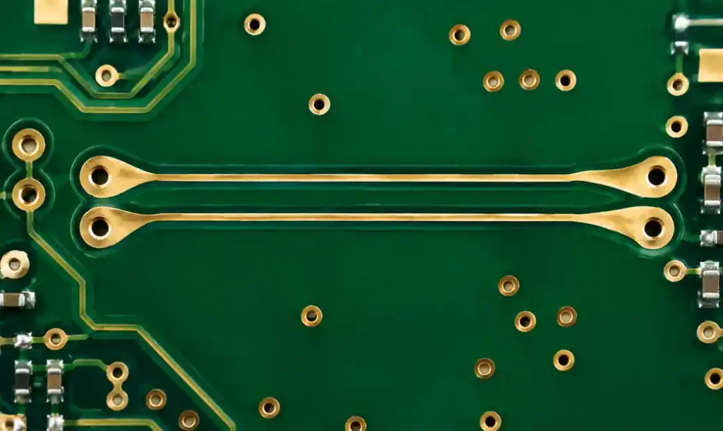
Automatic vs Manual Teardrop Implementation
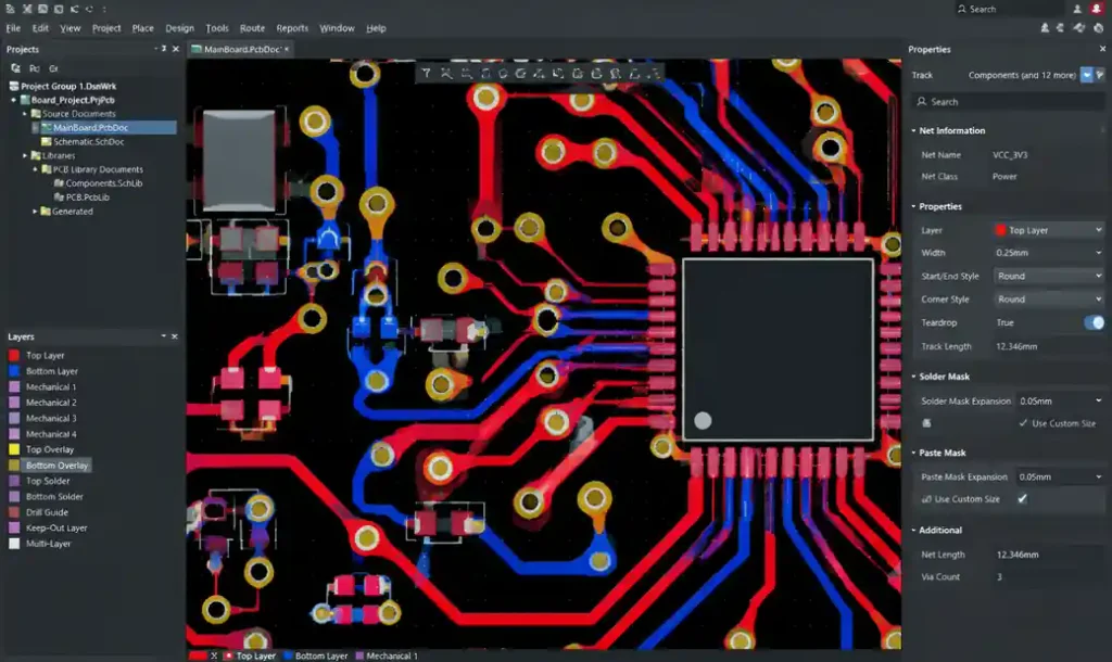
Modern PCB design software automates teardrop generation across entire layouts with rule-based controls. Altium Designer, Cadence Allegro, and KiCad offer batch teardrop commands that process thousands of connections in seconds. Automated systems ensure geometric consistency and eliminate human error in manual placement.
Design rules specify which connection types receive teardrops based on net class, layer, or component type. Power nets carrying >2A benefit from teardrops for current-handling capacity, while low-current signal nets may skip them to preserve routing density. Via types—through-hole, blind, buried—can have independent teardrop rules matching their mechanical stress profiles.
Manual teardrop placement remains necessary for complex geometries like staggered BGAs, tight differential pairs, and controlled impedance structures where automated tools produce routing violations. Skilled designers adjust teardrop parameters iteratively to balance reliability enhancement with routing completion and signal integrity requirements.
Dynamic teardrops update automatically when trace routes change during layout iterations. This prevents orphaned teardrop polygons that create design rule errors or unintended copper-to-copper shorts. Fixed teardrops offer stable geometry for final design review but require manual updates if routing changes late in the design cycle.
Impact on High-Frequency and Impedance-Controlled Designs
Teardrops create impedance discontinuities by locally widening the trace cross-section. A 0.15mm 50-ohm microstrip trace transitioning through a 0.5mm teardrop sees impedance drop to 35-40 ohms over 0.4mm length. For signals below 1 GHz, this 0.4mm discontinuity (0.001 wavelengths at 1 GHz) produces negligible reflection.
High-speed signals above 5 GHz require careful teardrop analysis. PCIe Gen 4 (16 Gbps), USB4 (40 Gbps), and DDR5 (6.4 Gbps) operate at frequencies where 0.3mm teardrop length represents 5-10% of signal wavelength. Time-domain reflectometry shows reflections from impedance mismatches exceeding 15% of characteristic impedance.
Differential pairs for HDMI 2.1, 10GbE, and MIPI interfaces require impedance-matched teardrops. Standard teardrops optimized for mechanical strength typically have 50-70% pad coverage, but this creates 8-12 ohm differential impedance variation. Reduced-coverage teardrops (20-30% pad area) limit impedance shift to <5 ohms while maintaining annular ring protection.
mmWave PCBs for 5G (24-40 GHz) and automotive radar (77 GHz) often omit teardrops entirely on RF traces. At these frequencies, any trace width discontinuity acts as a reactive element causing insertion loss and return loss degradation. Via transitions use back-drilling and controlled impedance via structures instead of teardrops for signal integrity.

Teardrop Implementation Checklist
Audit your design against IPC class requirements first. Class 3 mandates teardrops on all vias per IPC-6012, while Class 2 leaves implementation to designer discretion based on application environment. Document teardrop usage in fabrication notes to prevent fabricator modifications that introduce inconsistency.
Verify clearance violations after automatic teardrop generation. High-density layouts with 0.1mm trace spacing may experience copper-to-copper shorts where adjacent teardrops overlap. Design rule checks must include teardrop geometry in minimum spacing calculations.
Review high-speed nets individually for impedance impact. Run signal integrity simulations on critical interfaces like DDR memory, PCIe, and Ethernet to quantify reflection and insertion loss from teardrop discontinuities. Consider selective teardrop removal on nets where SI analysis shows unacceptable degradation.
Check teardrop orientation in flex zones. Dynamic flex areas require teardrops aligned perpendicular to bend direction to maximize stress relief. Parallel orientation concentrates bending stress along the teardrop edge, reducing effectiveness by 50-70%.
FAQ
Do teardrops increase manufacturing cost? No direct cost increase occurs since teardrops are part of the copper artwork. They may slightly increase design time if manual adjustment is needed, but automated generation minimizes labor.
Can teardrops cause signal integrity problems? Yes, in high-frequency designs above 5 GHz. Teardrops create impedance discontinuities that cause reflections. Careful sizing and selective application mitigate this risk.
Are teardrops required by IPC standards? IPC-6012 Class 3 requires teardrops for high-reliability applications. Class 2 does not mandate them, leaving the decision to designers based on application requirements.
Should I use teardrops on power planes? Power planes with >2A current benefit from teardrops for improved current capacity and mechanical strength at via connections. Low-current planes (<500mA) see marginal benefit.
How do teardrops affect routing density? Teardrops consume 15-25% more routing space around each via or pad. High-density designs may require selective teardrop application or smaller teardrop geometries to maintain routing completion.
Can I add teardrops after layout completion? Yes, modern EDA tools support batch teardrop generation on finished layouts. Review for clearance violations and manually adjust where automatic placement creates design rule errors.
Conclusion
PCB teardrops provide measurable reliability improvements in high-stress environments through mechanical reinforcement and annular ring protection. Class 3 applications, automotive electronics, and vibration-prone designs gain 60-80% reduction in connection failures with proper teardrop implementation.
However, teardrops are not universal requirements. Consumer electronics, low-cost IoT devices, and high-frequency RF designs often perform better without them due to routing constraints and signal integrity considerations. Base your decision on application environment, IPC class requirements, and specific failure modes relevant to your product’s operational profile.
Implement teardrops strategically using automated EDA tools with design rule controls, verify clearances post-generation, and document your approach in fabrication notes. This ensures manufacturing consistency and prevents reliability issues while maintaining signal integrity where needed.