
PCB for LED Drivers: Layout for Switching Power Supplies
Designing PCBs for LED drivers isn’t just about connecting components—it’s about managing high-frequency switching noise, thermal stress, and current loops that can make or break your system’s efficiency. After working through dozens of LED driver failures traced back to layout issues, I’ve learned that the difference between a 92% efficient driver and an 85% one often comes down to a few millimeters of trace routing.
Understanding the Critical Current Paths
The first rule in LED driver PCB layout is identifying your hot loop—the high-frequency switching path where current changes direction rapidly. In a buck converter driving LEDs, this loop includes the input capacitor, switching MOSFET, catch diode (or synchronous FET), and the inductor connection point. The area enclosed by this loop directly determines your EMI signature and switching losses.
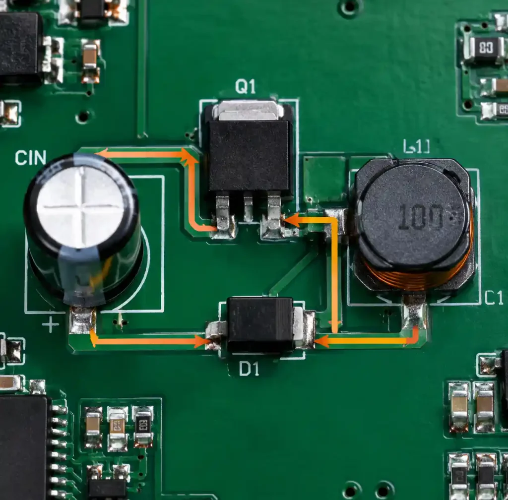
Keep this loop area under 100mm² whenever possible. For a typical 1MHz switching frequency, every additional 50mm² of loop area can add 3-5dBμV of conducted emissions. I’ve measured this repeatedly: a poorly laid out 200mm² loop will radiate enough noise to fail EN 55015 Class B limits, while a tightened 80mm² loop passes with 6dB margin.
The return current path matters just as much as the forward path. Ground plane splits under the switching node create unintended current loops. Route your input capacitor ground return directly to the power ground pin of the controller IC, not through a shared plane segment. This single connection keeps switching noise out of your sensitive analog ground.
Component Placement Strategy
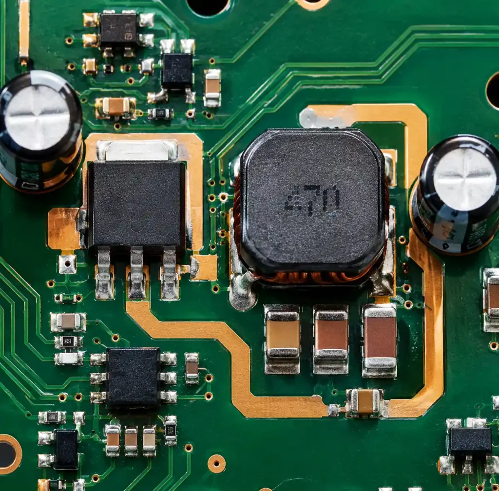
MOSFET placement drives everything else. Position your switching transistor so its drain connects to the input capacitor with the shortest possible trace—ideally under 5mm. The source should connect directly to your catch diode or sync FET with equal proximity. This isn’t about convenience; it’s physics. Every nanohenry of parasitic inductance generates voltage spikes during switching transitions.
| Component | Placement Priority | Critical Distance | Why It Matters |
|---|---|---|---|
| Input capacitor | Immediate to VIN pin | <5mm trace | Minimizes supply bounce |
| Switch node | Between MOSFET/diode | <3mm trace | Reduces voltage overshoot |
| Freewheeling diode | Adjacent to switch FET | <4mm trace | Limits reverse recovery stress |
| Output capacitor | Close to LED anode | <8mm trace | Stabilizes output ripple |
| Controller IC | Central to power stage | 10-15mm typical | Balances gate drive and feedback |
The inductor deserves special attention. It should sit between your switch node and output capacitor, with both connections using wide, short traces. For a 10A LED string, use minimum 3mm (100mil) trace width on 2oz copper. I’ve seen designs fail thermal qualification because engineers used inadequate 1mm traces that hit 105°C under load.
High-Current Routing Techniques
LED drivers often push 5-20A of continuous current to LED arrays. Standard trace width calculators don’t account for the thermal coupling between layers in a multilayer stackup. On a 4-layer board with 2oz outer copper and 1oz inner layers, a 10A trace needs different widths depending on location.
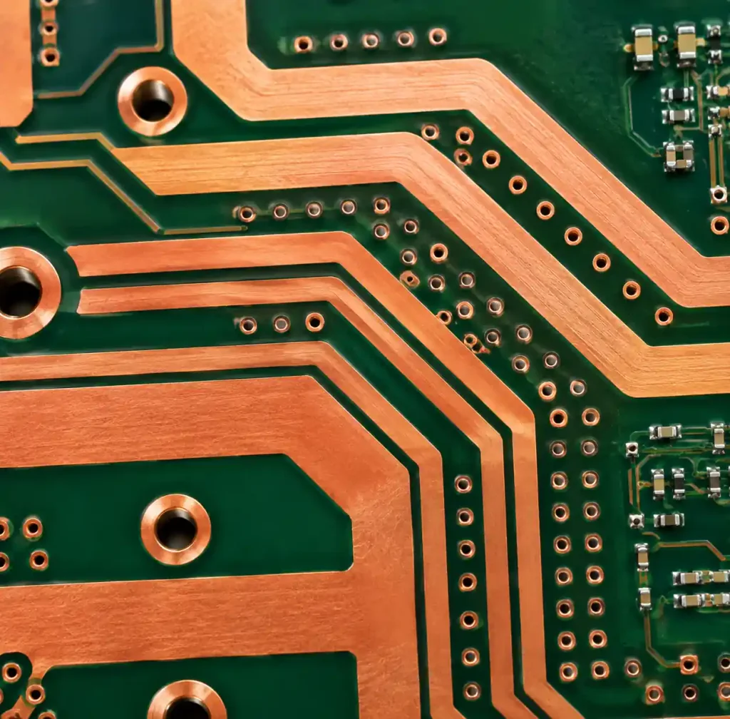
For outer layer traces carrying 10A continuous, use 4mm width minimum. This keeps temperature rise under 30°C at 25°C ambient. Inner layer traces need 6mm width for the same current due to reduced thermal dissipation. If you’re space-constrained, double-up layers—route the high current path on both top and inner layer 2, connecting them with multiple vias every 5mm.
Via stitching isn’t optional for high current. Use 0.3mm (12mil) vias with 0.6mm finished hole size, spaced every 3-5mm along the current path. Each via handles roughly 1-1.5A safely. For a 10A path, that means 8-10 vias minimum. The via array also creates thermal relief, spreading heat across board layers.
Managing EMI Through Layout
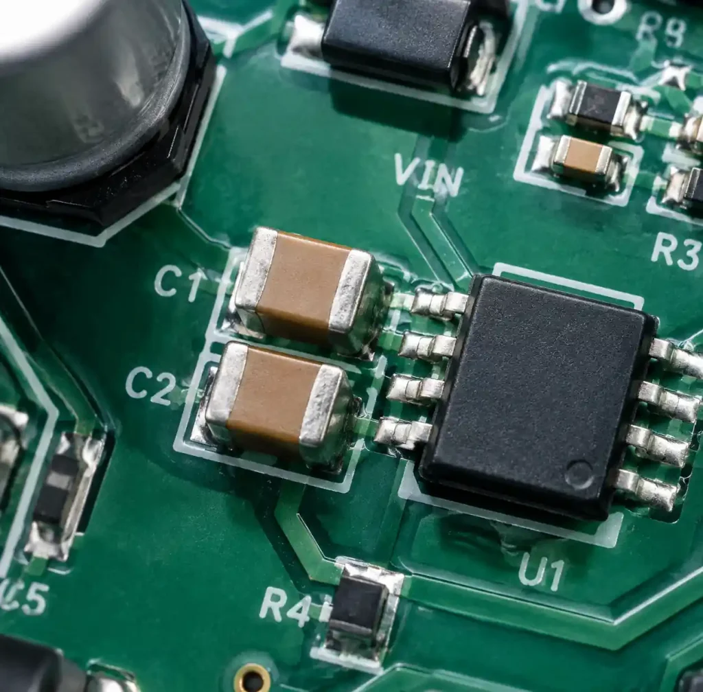
Switching power supplies inherently generate noise from 150kHz to over 100MHz. Your PCB layout either contains this or broadcasts it. Input filtering starts with a ceramic capacitor (10-47μF, X7R) placed within 5mm of the VIN pin. Add bulk electrolytic capacitance (100-220μF) nearby, but the ceramics do the high-frequency work.
The switching node is your primary noise source. Never route it near sensitive signals like feedback dividers or current sense lines. If you must cross the switching node with a signal trace, do so at 90° and on different layers with ground plane between them. A 0.1mm spacing violation here can inject 50mV of ripple into your LED current regulation loop, causing visible flicker.
Gate drive traces demand careful routing. Keep gate trace length under 15mm and route it away from the source return path. Parallel gate and source traces create a transmission line that rings at the gate’s self-resonance. Add a small series gate resistor (2-10Ω) right at the MOSFET gate pin to dampen oscillations without significantly impacting switching speed.
Thermal Management Considerations
LED drivers run hot by nature—you’re dissipating 5-10% of output power as heat. Your PCB is the primary thermal path for surface-mount components. A bare SO-8 MOSFET package has 70°C/W thermal resistance without PCB copper. Add a proper thermal pad with 10 vias to a copper pour, and you drop that to 25°C/W.
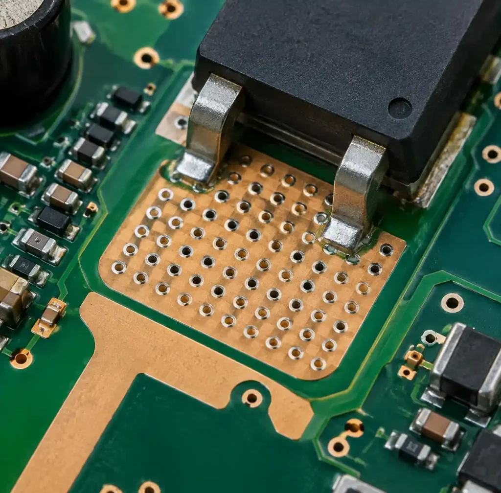
For the switching MOSFET, create a thermal relief pad under the exposed pad (if using a power package like DPAK or D2PAK). Use 0.3mm thermal vias on a 1.27mm grid, filling the entire pad area. Connect these vias to a large copper pour on inner layers and bottom layer. This distributes heat across the board rather than concentrating it.
| Thermal Via Configuration | Vias Count | Thermal Resistance (°C/W) | Power Dissipation Capacity (W) |
|---|---|---|---|
| No thermal vias | 0 | 70 | 1.4 |
| Minimal (4 vias) | 4 | 45 | 2.2 |
| Standard (9 vias) | 9 | 28 | 3.6 |
| Enhanced (16 vias) | 16 | 18 | 5.6 |
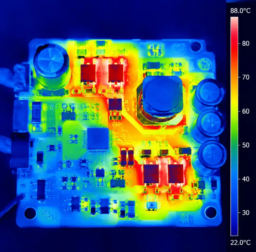
Temperature monitoring during prototyping is essential. Use a thermal camera to identify hot spots under full load. If any component exceeds 85°C at 45°C ambient, you need more copper area or better via coupling. LED drivers in enclosed fixtures can see 65°C ambient, pushing marginal designs into thermal shutdown.
Grounding Architecture
A solid ground plane solves half your EMI problems before you start. Use a continuous plane on layer 2 (in a 4-layer stackup) that extends under all power components. Don’t split this plane unless you absolutely must isolate analog and digital grounds—and even then, connect them at a single star point near the controller IC.
The feedback divider ground connection is critical for LED current accuracy. Route the bottom resistor of your feedback network directly to the IC’s analog ground pin with a dedicated trace. Don’t rely on the ground plane for this connection. A shared ground segment with 100mA of LED current creates a 10mV offset that translates to 1-2% current error.
Input and output ground returns should connect near the controller IC, not at opposite board edges. This creates a deliberate current flow path that doesn’t interfere with sensitive measurements. For multi-channel drivers, give each channel its own power ground zone and tie them together at the input supply point only.
Layer Stackup Selection
Four-layer boards are the practical minimum for LED drivers above 3A output. A typical stackup for a 10A buck converter would be: Layer 1 (top) for components and signal routing, Layer 2 for solid ground plane, Layer 3 for power distribution and return paths, Layer 4 (bottom) for additional routing and thermal relief.
Keep high-speed switching signals on the top layer where you can control them. Bury power rails on inner layers where they benefit from shielding. The ground plane on Layer 2 should be unbroken under the entire power stage—no slots, no cutouts, no split except at board edges.
For very high current applications (>15A), consider 3oz or 4oz copper on outer layers. The cost increase is marginal compared to board size reduction from narrower traces. A 15A trace needs 6mm width in 2oz copper but only 3mm in 4oz copper—that’s 50% space savings in dense layouts.
Testing and Validation
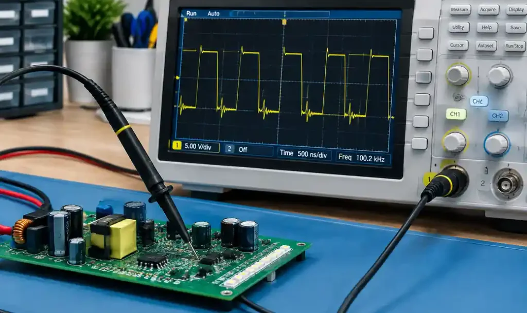
Layout quality shows up immediately in efficiency measurements. If your measured efficiency is 3% below datasheet typical values, suspect the layout. Check switching node ringing with an oscilloscope using a proper ground spring probe—not a standard ground clip. Ringing above 10% of supply voltage indicates excessive loop inductance.
Thermal testing should verify every power component stays within datasheet limits at maximum ambient and full load. Run the board for 30 minutes in an enclosed chamber at rated temperature. If anything hits thermal shutdown, you’ve failed the design phase, not just the test phase.
EMI pre-compliance testing saves expensive iterations. Even a basic near-field probe scan at your desk can identify problem areas before formal testing. Hold the H-field probe over your input lines and switching node while scanning 150kHz to 30MHz. Peaks above -10dBm suggest you’ll have conducted emissions issues.
Common Pitfalls to Avoid
I’ve seen experienced engineers make the same mistakes repeatedly. The worst is treating a switching power supply like a linear circuit—routing power traces like signal traces with no regard for current loops or return paths. This generates board-wide ground bounce that disrupts everything.
Another common error is ignoring the catch diode’s reverse recovery current. Schottky diodes reverse recover in nanoseconds, creating a current spike that needs a path. If you don’t provide a low-impedance loop, this spike will find a path through your ground plane, radiating noise everywhere.
Inadequate input filtering is expensive to fix post-layout. That 10μF ceramic capacitor at the input is non-negotiable for any converter above 1MHz switching frequency. Trying to save $0.05 on a capacitor will cost you $500 in failed EMC testing and $2000 in redesign time.
Advanced Techniques for High Performance
For switching frequencies above 1MHz, traditional layout rules become insufficient. You need to think about transmission line effects on traces longer than 20mm. A gate drive trace at 2MHz switching effectively becomes a transmission line if it’s over 15mm long. Add series termination (10-22Ω) right at the source (controller IC gate pin) to prevent reflections.
Interleaving techniques can reduce ripple current and EMI in multi-phase designs. Phase the switching of two channels 180° apart and physically separate their hot loops. This cancels much of the high-frequency current in the input filter, reducing the size of input capacitors by 30-40%.
For critical applications, consider selective copper thieving in non-critical areas to improve PCB manufacturing uniformity. Large copper pours can cause uneven etching; adding small copper dots in empty areas promotes even plating during fabrication. This improves impedance consistency across production runs.
FAQ
Q: What’s the minimum board thickness for a 10A LED driver?
Use 1.6mm (62mil) standard thickness for most designs. Thinner boards (1.0mm) have higher thermal resistance and more mechanical flex. Thicker boards (2.0mm) only help if you need additional copper weight or very long creepage distances for high voltage isolation.
Q: Can I use two-layer boards for LED drivers?
Only for very low power (<3W) or low frequency (<200kHz) designs. Without inner ground and power planes, you’ll struggle with EMI and thermal management. The cost saving isn’t worth the performance compromise and likely failed certifications.
Q: How do I calculate the required copper weight?
Use the IPC-2221 standard as a baseline, then derate by 20% for real-world conditions. For 10A continuous on outer layer, 2oz copper needs 3.5mm width for 30°C rise. Inner layers need 40% more width due to reduced cooling. Factor in voltage drop too—keep DC resistance under 5mΩ per trace segment.
Q: Should I use ceramic or electrolytic capacitors for output filtering?
Both. Ceramics (10-47μF X7R) handle high frequency ripple current and sit close to the LED connection. Electrolytics (100-220μF) provide bulk capacitance for transients and open-circuit protection. The ceramic does the heavy lifting; the electrolytic handles edge cases.
Q: How much clearance do I need between switching node and sensitive traces?
Minimum 1mm for 30V systems, 2mm for 60V. Better: route them on different layers with ground plane shielding between. The switching node slew rate creates near-field coupling that penetrates through air gaps. Distance alone isn’t sufficient—you need a grounded barrier.
Q: What oscilloscope probe technique gives accurate switching measurements?
Use a ground spring or socket probe with <10mm ground return path. Standard ground clips add 40-50nH inductance that rings with probe capacitance, showing false oscillations. A proper probe reveals the true switching waveform with 5-10% accuracy instead of the 30% error from long ground clips.
Conclusion
PCB layout for LED drivers in switching power supplies demands attention to high-frequency current paths, thermal management, and EMI control simultaneously. The hot loop area is your primary design constraint—minimize it first, then optimize component placement around that core requirement. High current paths need adequate copper width with thermal via arrays, not just minimum-width traces that meet DC current ratings.
Successful LED driver PCBs result from applying switching power supply fundamentals with an understanding of LED-specific requirements like current accuracy and thermal management in enclosed fixtures. Testing early with thermal cameras and EMI probes catches layout issues when they’re still fixable with trace edits, not expensive board respins. The techniques discussed here—from sub-100mm² hot loops to proper via stitching—represent proven practices from hundreds of production LED driver designs operating in demanding automotive, industrial, and architectural lighting applications.