PCB function test:the key steps to ensure the reliability of electronic device
Introduction
In the modern electronic devices manufactures process,print circuit board as the carrier of component device, its quality and reliability can directly impact the performance of whole device,In order to ensure that the pcb can work properly after assembly,functional test has became an integral part of the production process.This article will delve into the purpose、method、process、challenges、and future trends.
1.Purpose of pcb function test
The main purpose of pcb function test is to verify that the various circuits and components on the pcb board work normally in accordance with the design requirements.Through the function test,it can ensure that the pcb can perform its intended function before it is assembled into the final product.
2.Method of pcb function test
pcb function test include these :
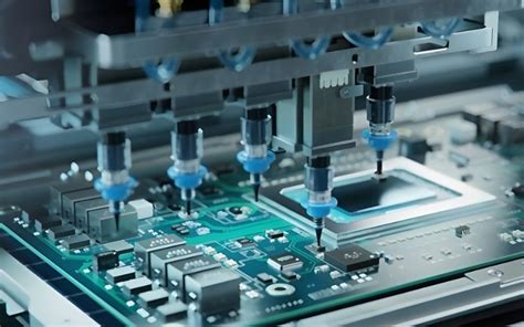
(1)In-Circuit test (ICT):contact the test point on the pcb through the test pcb probe,check the electrical performance and connection of each component if correctly.
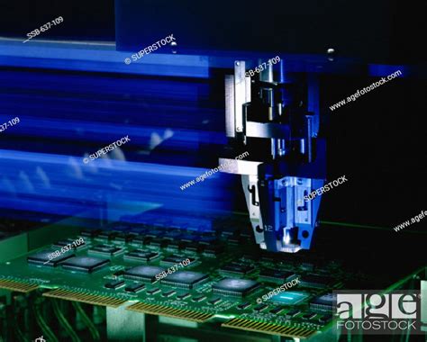
(2)Flying probe Test:Non-fixed contact testing using a moving probe, suitable for small batch or high mixing production environment.
(3)Boundary Scan Test:Test digital circuits on PCBs using the test access port (TAP) and boundary scan registers defined by the IEEE 1149.1 standard.
(4)Functional test:Simulating the reality working condition,complete function,verification of PCB.Ensure its performance in practical application.
3.Process of pcb functional test
the process of the pcb functional test including these steps:
(1)Test planing:according to the pcb design specification and function requirement,developing detailed test plan and test cases.
(2)Test fixture design:test fixture designed to hold PCBS and provide electrical connections
(3)Test program development:Write software programs that control test equipment and execute test cases
(4)Test execute:Install the pcb onto text fixture,run test program,recording test results.
(5)Result analysis: analysis the test result,ensure the pcb if pass the test,or further debugging and repair.
(6)test report: Write text pcb report.Record key data and problems found during the testing process.Record key data and problems found during the testing process.
4.PCB function test and challenge
pcb function test faced the main challenge include:
(1).Complexity increase: with the electronic device function increase, pcb design become more complex,the difficulty of test is also increase.
(2)Test cover rate:ensuring that testing covers all critical functions and potential points of failure is achallenge.
(3)Cost control: High-performance test equipment and complex test procedures may lead to rising costs.
(4)Time pressure: In a rapidly changing market, shortening the time to market is the key, and the test process needs to be efficient and fast.
5.Future development trends of PCB functional testing
With the advancement of technology, PCB functional testing is also developing. Future trends include:
Automated testing: Improve test efficiency and accuracy through automated test equipment and software.
Intelligent testing: Use artificial intelligence and machine learning technology to optimize test processes and fault diagnosis.
Remote testing: Remote monitoring and control of the test process through network technology.
Sustainability testing: Develop environmentally friendly test methods and materials to reduce environmental impact during testing.
Conclusion
PCB functional testing is a key step in ensuring the reliability of electronic equipment. With the continuous increase in the functions of electronic equipment and the rapid changes in the market, PCB functional testing faces new challenges and opportunities. Through continuous technological innovation and process optimization, PCB functional testing will continue to provide solid guarantees for the quality and reliability of electronic equipment.


