
PCB Layer Stackup Design: Complete Guide for Signal Integrity
If you want to design high-speed PCBs with reliable signal integrity, you need to understand layer stackup configuration, impedance control, return path management, and power distribution strategies that prevent electromagnetic interference and signal degradation. PCB layer stackup design is one of the most critical decisions in high-speed circuit board development. Poor stackup choices account for up to 60% of signal integrity failures in products operating above 100 MHz, leading to costly redesigns and production delays.
This guide explains stackup design principles, layer arrangement strategies, impedance calculation methods, and design rules that experienced PCB engineers use to achieve reliable signal integrity in multilayer boards.
What Is PCB Layer Stackup Design?
PCB layer stackup design is the process of arranging signal, ground, and power layers in a multilayer board to achieve specific electrical performance, mechanical properties, and manufacturing requirements. The stackup defines the sequence of copper layers, dielectric materials, thicknesses, and dielectric constants that determine impedance, signal integrity, and electromagnetic compatibility.

A typical stackup specification includes layer type designation, copper weight (0.5oz to 2oz), dielectric material selection, and core/prepreg thicknesses. Stackup design directly impacts signal rise times, crosstalk, EMI, and manufacturing yield. Complete stackup design early in the layout process—changing it after routing begins requires complete redesign.
Why Stackup Design Matters for Signal Integrity
Signal integrity depends on how signals interact with their reference planes and adjacent traces. Proper stackup design ensures every high-speed signal has a continuous, low-impedance return path and maintains controlled impedance throughout the transmission line.
When signals transition between layers through vias, discontinuities in the return path create impedance changes that reflect signal energy, distort waveforms, and radiate EMI. A well-designed stackup minimizes these discontinuities by placing signal layers adjacent to solid reference planes.

High-speed digital signals above 100 MHz behave as transmission lines where impedance matching becomes critical. Typical controlled impedance targets are 50Ω for single-ended signals and 90Ω or 100Ω for differential pairs, with tolerances of ±10% or ±5Ω per IPC-2141.
Core Stackup Design Principles
Adjacent Reference Planes: Every signal layer should be adjacent to at least one solid reference plane (ground or power). This provides a short return path, reduces loop area, and creates natural electromagnetic shielding. Avoid placing two signal layers adjacent without an intervening reference plane—this creates strong crosstalk coupling.
Symmetrical Stackup: Place copper layers symmetrically about the board centerline to balance copper distribution and prevent warping during manufacturing. Asymmetric copper distribution creates unequal thermal expansion that bends boards during reflow soldering, especially in lead-free processes reaching 260°C peak.
Tight Coupling: Place signal layers close to their reference planes (3-6 mils or 75-150μm) for high-speed signals above 500 MHz. Closer spacing reduces loop area for return currents, directly reducing EMI. Tight coupling also increases capacitance per unit length, providing better high-frequency bypass.
Multiple Ground Planes: Additional ground planes provide redundant return paths, reduce ground bounce, offer shielding between signal layers, and lower AC impedance of the ground distribution network.

For boards with both high-speed digital and sensitive analog circuits, dedicate separate ground planes to each circuit type and connect them at a single point or through ferrite beads.
Common Layer Stackup Configurations
4-Layer Stackup (up to 500 MHz):
- Layer 1 (Top): Signal + components
- Layer 2: Ground plane (solid)
- Layer 3: Power plane (solid or split)
- Layer 4 (Bottom): Signal + components
Route high-speed signals on the top layer where possible, as this layer has the tightest coupling to its reference plane. Achieve 50Ω impedance with trace widths of 8-12 mils depending on dielectric thickness.
6-Layer Stackup (200 MHz to 2 GHz):
- Layer 1 (Top): Signal
- Layer 2: Ground plane (solid)
- Layer 3: Signal (orthogonal to Layer 1)
- Layer 4: Signal (orthogonal to Layer 5)
- Layer 5: Ground plane (solid)
- Layer 6 (Bottom): Signal
All signal layers stay tightly coupled to ground planes. Route power distribution on Layers 3 and 4 using flood fills between signal traces. Excellent for DDR3/DDR4, Gigabit Ethernet, USB 3.x, and PCIe Gen 2/3.
8-Layer Stackup (multi-gigabit designs):
- Layer 1 (Top): Signal
- Layer 2: Ground plane (solid)
- Layer 3: Signal (stripline)
- Layer 4: Power plane (multiple rails)
- Layer 5: Ground plane (solid)
- Layer 6: Signal (stripline)
- Layer 7: Ground plane (solid)
- Layer 8 (Bottom): Signal
Provides stripline routing on Layers 3 and 6 between two reference planes for superior shielding. Symmetrical arrangement prevents warping. Use for PCIe Gen 3+, 10G Ethernet, USB4, DDR4/DDR5, or strict EMI requirements per CISPR 32 Class B or FCC Part 15.

Impedance Control in Stackup Design
Microstrip vs Stripline
Microstrip places the signal trace on an outer layer with one reference plane below. Asymmetrical field distribution (air above, dielectric below) makes microstrip impedance higher than stripline for equivalent trace widths.
Stripline places the signal trace between two reference planes, completely surrounded by dielectric. Symmetrical field distribution provides better impedance control (±5% vs ±10%), lower loss, and superior EMI shielding.
Common Impedance Targets
| Interface Type | Impedance | Tolerance | Topology |
|---|---|---|---|
| DDR3/DDR4 Memory | 40Ω, 50Ω | ±10% | Single-ended |
| DDR5 Memory | 40Ω | ±10% | Single-ended |
| USB 2.0 | 90Ω | ±10% | Differential |
| USB 3.x/4 | 90Ω | ±10% | Differential |
| PCIe (all generations) | 85Ω | ±10% | Differential |
| Ethernet 10/100/1000 | 100Ω | ±10% | Differential |
| HDMI/DisplayPort | 100Ω | ±10% | Differential |
| LVDS | 100Ω | ±10% | Differential |
Design your stackup to accommodate the most restrictive impedance requirement, then adjust trace widths for other impedances.
Return Path Management
High-frequency signal currents travel outward on the signal trace and return through the nearest reference plane directly beneath the trace. Managing these return paths is critical for signal integrity and EMC.
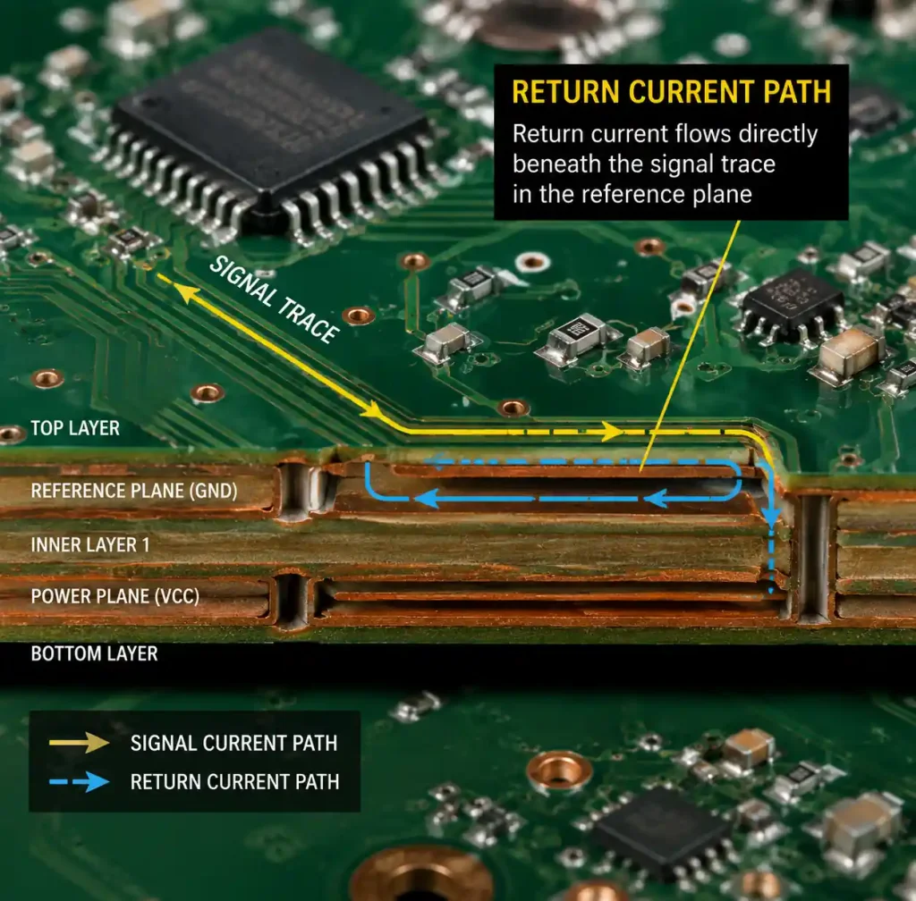
Continuous Reference Planes: Maintain unbroken reference planes beneath high-speed traces. Any gap forces return currents to detour, increasing loop area, radiating EMI, and creating impedance discontinuities. Avoid routing high-speed traces over gaps between split power planes. If crossing is unavoidable, place ground stitching vias within 20-50 mils of the gap.
Via Return Path Transitions: When signals change layers, return currents must also transition between reference planes. Place ground return vias within 20 mils of signal vias for signals above 1 GHz. For differential pairs, place one ground via between the pair’s signal vias to maintain return path symmetry.
Reference Plane Changes: Avoid changing reference plane type (ground to power) for high-speed signals. If unavoidable, place multiple bypass capacitors (0.1μF or 1μF) near the via transition point.
Power Distribution Network Design
Power and Ground Plane Pairing: Place power and ground planes adjacent with thin dielectric spacing (2-5 mils). This creates 50-300 pF per square inch of distributed capacitance. This provides high-frequency energy storage for transient currents that discrete capacitors cannot provide above 50-100 MHz.
Multiple Power Rails: For boards with multiple voltages, split power planes into separate copper areas. Maintain at least 20 mils clearance between different voltage areas. Never route high-speed signals across gaps between split power planes.
Common Stackup Design Mistakes
Mistake 1: Inadequate Reference Planes. Too few ground planes or signal layers far from reference planes create poor impedance control and EMI. For designs above 500 MHz, ensure every signal layer is directly adjacent to a solid reference plane.
Mistake 2: Asymmetric Copper Distribution. Unbalanced copper causes board warping during reflow, creating assembly defects for fine-pitch components. Design symmetrical stackups and target less than 10% copper area difference between mirrored layers.
Mistake 3: Split Planes Under High-Speed Signals. Routing signals over gaps in split power planes forces return currents to detour, creating EMI and reflections. Never route signals faster than 50 MHz over plane splits. If unavoidable, place ground stitching vias every 100-200 mils.
Mistake 4: Ignoring Manufacturing Constraints. Specifying dielectric thicknesses or impedance beyond manufacturer capabilities leads to redesigns. Consult your PCB fabricator early to verify achievable values and request impedance test coupons.
Mistake 5: Insufficient Layer Count. Routing complex high-speed designs on inadequate layers forces compromises in signal quality and power distribution. The cost difference between 6-layer and 8-layer boards (30-50%) is far less than redesign costs. Andwin Circuits offers multilayer PCB manufacturing up to 50 layers.

FAQs
What is the minimum layer count for controlled impedance PCB design?
Four layers is the practical minimum using Signal-Ground-Power-Signal arrangement, supporting designs up to 500 MHz. Higher speed applications above 1 GHz typically require 6 or more layers.
Should I use microstrip or stripline for high-speed signals?
Stripline offers superior performance for critical high-speed signals due to better impedance control (±5%), lower EMI, and reduced susceptibility. Use stripline for signals above 1 GHz, differential pairs for high-speed serial links, and sensitive clock networks.
How thick should the dielectric be between power and ground planes?
Target 2-5 mils (50-125μm) spacing to create 100-300 pF per square inch of plane capacitance. Verify achievable thicknesses with your fabricator.
What stackup is best for PCIe Gen 4 or Gen 5 applications?
8-layer or higher with stripline differential pair routing on 85Ω impedance, ±10% tolerance. Use low-loss dielectric materials (Dk=3.8-4.2, Df<0.01) rather than standard FR-4 to minimize insertion loss at multi-gigahertz frequencies.
Can I route signals on the same layer as a power plane?
Yes, for low-speed control signals. Maintain 20-40 mils clearance between signal traces and power plane copper areas. Avoid routing high-speed signals on split power planes where return path discontinuities degrade signal integrity.
Conclusion
PCB layer stackup design directly determines signal integrity performance, electromagnetic compatibility, and manufacturing reliability for modern high-speed electronic products. Proper configuration with adequate reference planes, controlled dielectric spacing, and balanced copper distribution prevents signal integrity failures. The key principles—adjacent reference planes for all signal layers, symmetrical copper distribution, tight coupling between signals and planes, and continuous return paths—apply across all layer counts and applications.
If you need high-quality multilayer PCBs with precise impedance control, Andwin Circuits offers advanced manufacturing up to 50 layers with fast turnaround in 7 days, certified to ISO 9001, IATF 16949, and UL standards. We provide impedance testing per IPC-2141 within ±5Ω tolerance and have manufactured complex stackups for automotive, 5G telecom, medical devices, and high-performance computing worldwide.
Contact us today for custom PCB stackup design consultation and competitive factory-direct pricing.