
PCB Panelization Guide: Optimize Manufacturing Cost and Efficiency
If you want to cut assembly cost and lift SMT yield, then you need to master PCB panelization before your Gerber files ever reach the fab.
Panelization decides how many boards ride through a reflow oven per pass, how much laminate you scrap, and whether components crack at depaneling. On a busy SMT line, a single panel that carries 8 boards instead of 1 spreads fixed setup cost, feeder loading, and oven time across every unit. Get the layout wrong and you pay for warpage, edge cracking, and stalled placement machines that cannot grip an undersized board.
This guide covers array layouts, breakaway methods, fiducials, tooling holes, panel-size standards, and depaneling design, with the exact numbers our engineers use daily.
What Is PCB Panelization?
PCB panelization is the practice of arranging multiple identical (or mixed) boards on one larger manufacturing panel, also called an array. The fab builds, tests, and assembles the whole panel as a single unit, then separates the individuals afterward.
The reason is economics. Placement machines, stencils, and reflow profiles are set up once per panel, not once per board. A well-built array can raise line throughput 3-8× and improve first-pass yield, because small or odd-shaped boards stay rigid and dimensionally stable through PCB assembly.
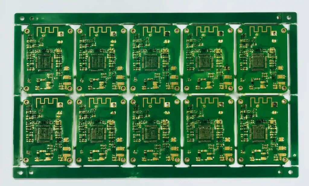
Panel Anatomy: Rails, Fiducials, Tooling Holes
Every production panel needs a border frame that the SMT conveyor and pick-and-place system can grip. This is where most first-time designs fail.
Breakaway rails run along the panel edges to carry fiducials and tooling holes. Rails of 5-10 mm are standard; go below 5 mm and the panel flexes during placement. Keep at least 3 mm of component keepout from any rail or score line so parts survive separation.
Fiducials are copper reference marks the vision system uses to align the stencil and nozzles. Use 1 mm solid copper dots with a 2 mm bare solder-mask clearance ring. Place three global fiducials on the panel rails in an asymmetric L-pattern so the machine detects orientation, plus local fiducials near fine-pitch BGAs.
Tooling holes (non-plated, typically 3.0-3.175 mm) locate the panel on assembly fixtures and depaneling jigs. Add at least two, diagonally opposite, on the rails.
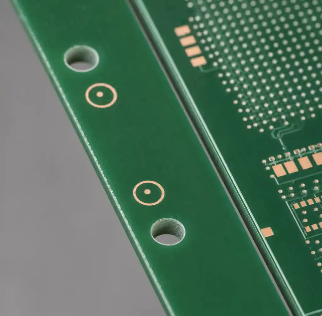
Breakaway Methods: V-Cut vs Mouse Bites vs Tab Routing
The separation method is the single biggest DFM decision in a panel. It sets edge quality, mechanical stress, and how tightly you can pack boards.
V-Cut (V-scoring) cuts a 30° groove into the top and bottom faces, leaving a thin web of 0.3-0.4 mm. It only works for straight, edge-to-edge lines on rectangular boards. Boards can butt together at 0 mm spacing, giving the best material utilization.
Mouse bites (stamp holes) are rows of small drilled holes (0.5 mm) along a breakaway tab, spaced roughly 0.3-0.4 mm apart. They handle irregular outlines and let you place tabs only where the board is strong.
Tab routing mills a slot around each board, leaving solid tabs (often reinforced with mouse bites) that break away later. It suits non-rectangular shapes and gives clean routed edges.
| Factor | V-Cut | Mouse Bites | Tab Routing |
|---|---|---|---|
| Board shape | Rectangular only | Any shape | Any shape |
| Edge quality | Clean, straight | Rough nubs | Clean (routed) |
| Board spacing | 0 mm | 1.6-2.0 mm | 2.0-2.4 mm |
| Material use | Highest | Medium | Lowest |
| Depanel stress | Low (with tool) | Higher | Lowest |
| Best for | High-volume rigid | Small/odd boards | Complex outlines |
A field note from our floor: continuous V-score lines transmit bending stress across the whole row, so V-cut is risky near ceramic capacitors placed close to the edge. For high-reliability builds, we prefer tab routing with mouse bites because it isolates stress to discrete tabs instead of a long weakened score line.
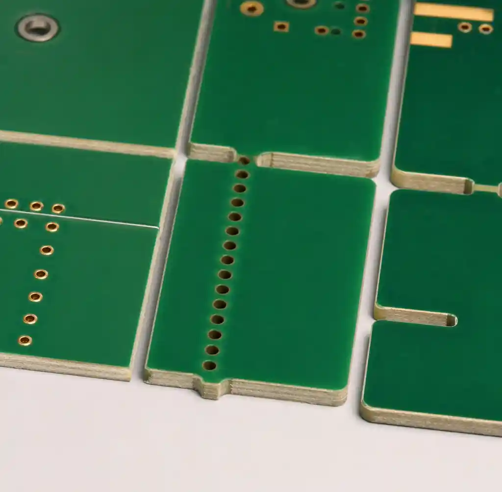
Panel Size Standards and Utilization
Working panels are sized to the fab’s process equipment, not to your board. Choosing a size that nests cleanly into standard laminate sheets is where real cost savings hide.
| Panel Size (mm) | Panel Size (in) | Typical Use |
|---|---|---|
| 305 × 457 | 12 × 18 | Common SMT standard |
| 457 × 610 | 18 × 24 | High-volume production |
| 254 × 305 | ~10 × 12 | Small-batch / prototype |
Aim for panel utilization above 75-80%. Utilization is the total board area divided by the full panel area, including rails and gaps. To raise it, rotate or mirror boards to fill corners, use V-cut where shapes allow, and keep rails no wider than needed. Every wasted square centimeter of FR-4 or metal core PCB is laminate you paid for and scrapped.
Metal core boards deserve special care. Aluminum substrates cannot be V-scored cleanly the way FR-4 can, so MCPCB panelization usually relies on routing with tabs or laser cutting to protect the dielectric layer.
Design for Depaneling
How you separate boards after assembly determines whether solder joints survive. Match the depaneling method to your components early, during panel design.
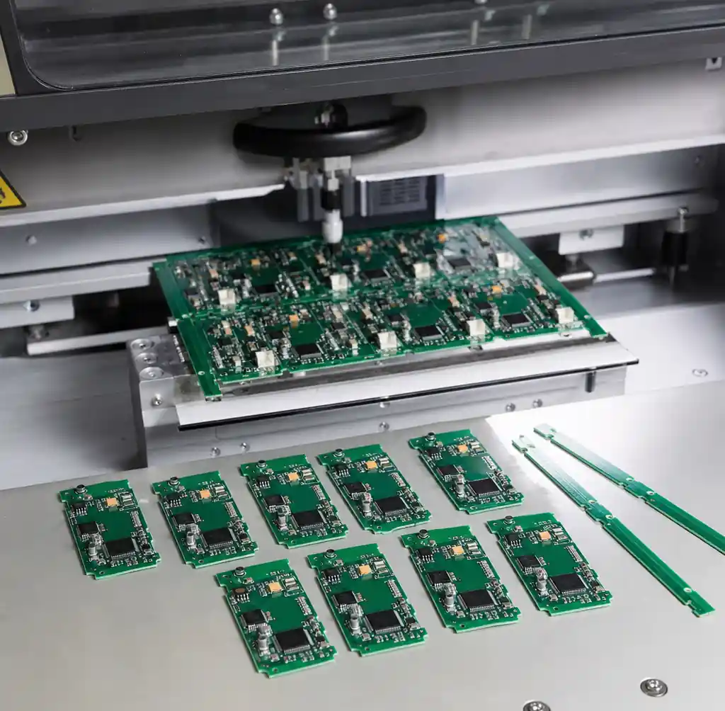
Three methods dominate, and each trades stress against cost and outline freedom.
| Method | Mechanical Stress | Outline Freedom | Relative Cost |
|---|---|---|---|
| Manual (pizza cutter) | High (bending) | Straight V-scores only | Lowest |
| Router (CNC) | Low | Any shape | Medium |
| Laser | Lowest | Any shape, tight arrays | Highest |
Manual separation works for straight V-scores but bends the board, so keep sensitive parts away from the score. Router (CNC) depaneling cuts tabs with minimal stress and handles any outline. Laser depaneling delivers the lowest mechanical stress and cuts fine, tight arrays; leave about 0.1 mm clearance to compensate for laser and placement accuracy.
Design rules that prevent scrap: keep tall or heavy components 3 mm minimum from break lines, orient BGAs and ceramic caps parallel to the score to avoid flex-induced cracks, and never route board-critical traces through a mouse-bite tab. For flexible and rigid-flex PCB arrays, laser cutting is often the only stress-safe option.
How to Calculate Panel Cost
Panel cost per board is not just laminate. Start from the working panel area, subtract rails and gaps to get usable area, then divide by your board footprint to find the “up count” (boards per panel).
Cost per board drops as up count rises, because NRE, tooling, stencil, and setup are fixed per panel. But there is a break-even: pushing spacing too tight raises depaneling stress and scrap, wiping out the savings. Balance up count against utilization and yield.
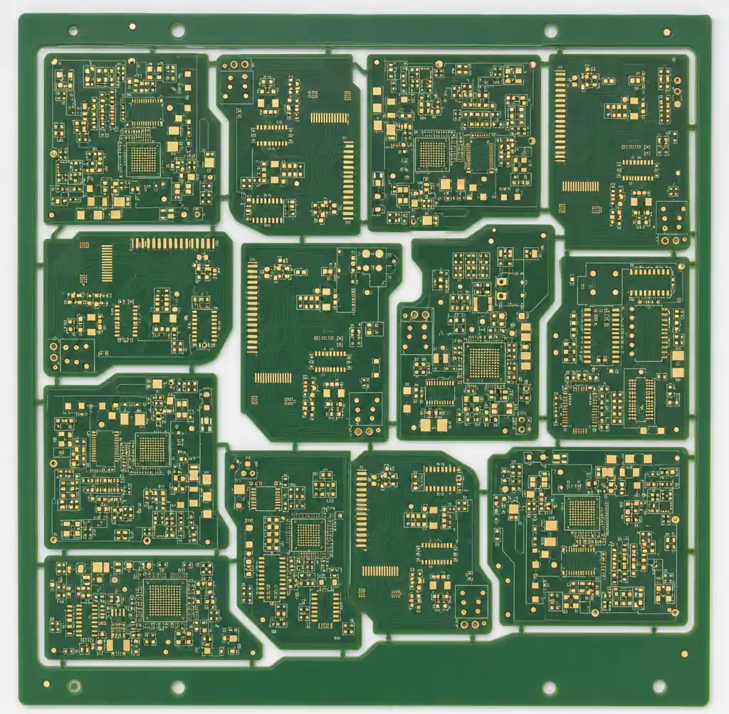
A practical workflow: get your board footprint, pick the fab’s standard panel size, model 2-3 array layouts, and compare cost per good board (not cost per panel). This is where a manufacturer’s DFM review pays for itself before you commit to PCB manufacturing.
FAQs
What is the minimum spacing between boards for V-scoring?
V-scored boards can butt directly together at 0 mm spacing because the groove replaces the gap. For mouse bites, allow 1.6-2.0 mm between boards for the tab and router bit.
How many boards should I put on a panel?
Enough to reach 75-80%+ utilization without dropping below 5 mm rails or 3 mm component keepout. Higher up counts cut per-board cost but only if yield holds during depaneling.
Where do fiducial marks go on a panel?
Place three 1 mm global fiducials in an asymmetric pattern on the rails for panel-level alignment, plus local fiducials beside fine-pitch parts like BGAs and QFNs.
Can metal core PCBs be panelized like FR-4?
Not with V-scoring. Aluminum and copper substrates are routed with tabs or laser-cut, since scoring damages the thermal dielectric. See MCPCB panelization for details.
Which depaneling method causes the least stress?
Laser depaneling produces the lowest mechanical stress, followed by router cutting. Manual snapping of V-scores creates the most bending, so it needs generous component keepout.
Conclusion
PCB panelization is where design intent meets factory reality. The right array layout raises SMT throughput several-fold and spreads fixed cost across many boards, while the wrong breakaway choice invites warpage, cracked joints, and wasted laminate. Choose V-cut for rectangular high-volume boards, mouse bites for small or odd shapes, and tab routing or laser cutting for complex and stress-sensitive assemblies. Target 75-80%+ utilization, use 5-10 mm rails, three global fiducials, and 3 mm component keepout as your baseline.
If you need expert panelization for FR-4, metal core PCB, or rigid-flex arrays, Andwin Circuits offers up to 50-layer manufacturing with free DFM review and fast delivery in 7 days, backed by ISO 9001 and IATF 16949 certification.
Contact us today for custom panelization, DFM optimization, and competitive factory-direct pricing.