
PCB Reverse Engineering: Legal Considerations and Technical Process
Reverse engineering accounts for approximately 15-20% of PCB analysis work in the electronics industry. This process involves reconstructing circuit board designs from physical products, particularly for obsolete component replacement, failure analysis, and design validation.
If you need to extract PCB schematics from legacy products or analyze competitor designs for your electronic device project, then you will need to understand the legal framework, technical methods, and ethical boundaries of PCB reverse engineering.
What is PCB Reverse Engineering?
PCB reverse engineering is the systematic process of analyzing a physical printed circuit board to extract its schematic, component specifications, and interconnection netlist. Engineers use this methodology to recreate design files when original documentation is unavailable or when investigating circuit functionality for legitimate purposes.
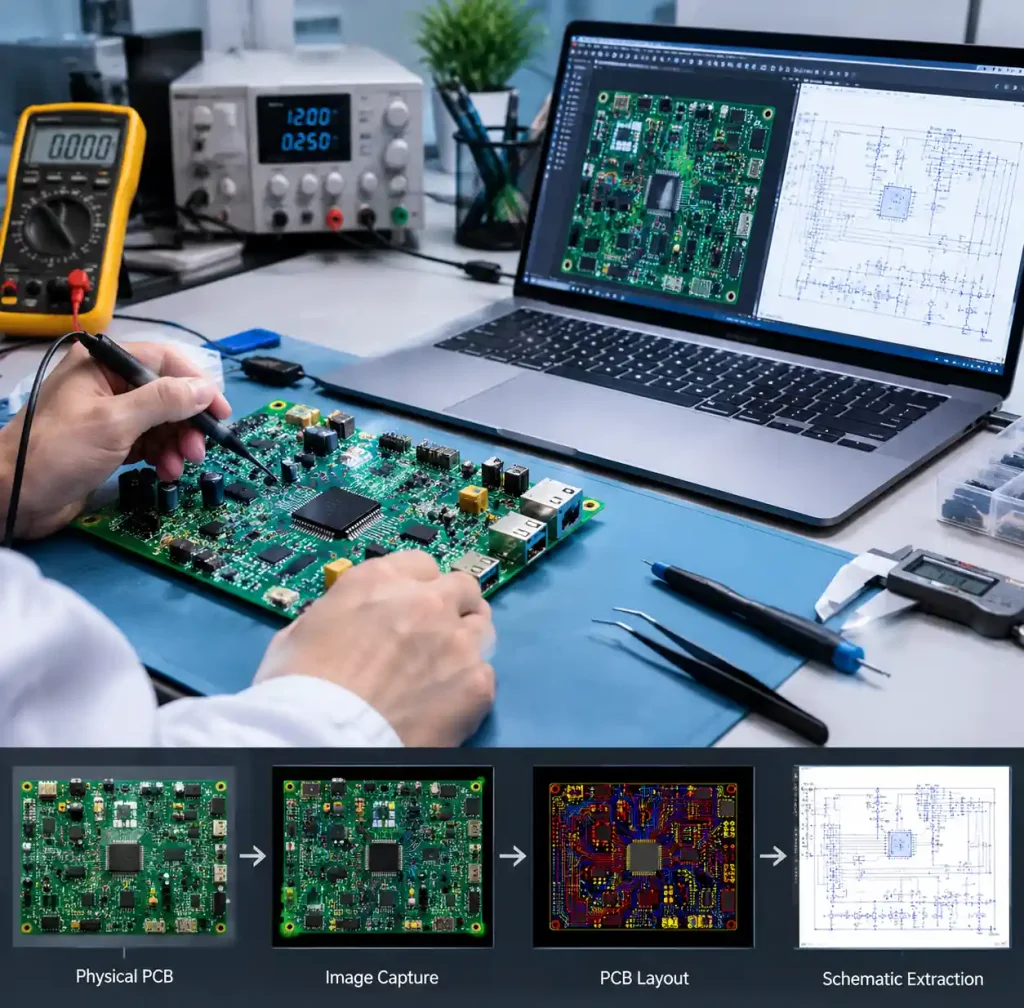
The process reconstructs board layouts through non-destructive and destructive testing methods. X-ray imaging reveals internal layer structures without damaging the PCB, while microsectioning provides cross-sectional analysis of via connections and layer stackup. Modern automated tools can extract netlists from high-resolution board images to generate CAD files compatible with design software.
You can apply PCB reverse engineering for obsolete product support, failure analysis investigations, and interoperability research when original manufacturers discontinue support or documentation.
Legal Framework for PCB Reverse Engineering
Intellectual Property Considerations
PCB designs receive protection under copyright law, trade secret statutes, and occasionally patent rights depending on jurisdiction. In the United States, the fair use doctrine permits reverse engineering of lawfully purchased products for specific purposes including interoperability, education, and security research.
According to trade secret law, reverse engineering is broadly legitimate when the product was obtained through legal channels. The Digital Millennium Copyright Act (DMCA) Section 1201(f) explicitly allows circumvention of access controls for interoperability purposes, provided the information cannot be readily obtained elsewhere.

When Reverse Engineering is Legitimate
| Purpose | Legal Status | Requirements |
|---|---|---|
| Obsolete Product Support | Permitted | Original product no longer manufactured or supported |
| Failure Analysis | Permitted | Owner of defective product seeking root cause |
| Interoperability Research | Permitted | Necessary for compatible product development |
| Security Analysis | Permitted | Good-faith vulnerability research |
| Component Identification | Permitted | Identifying parts for repair or replacement |
| Design Cloning | Prohibited | Copying for competitive reproduction |
| Patent Infringement | Prohibited | Replicating patented circuit topologies |
European Union’s Copyright Directive Article 6 provides similar protection for reverse engineering conducted for interoperability purposes. However, you must obtain products through legal purchase rather than unauthorized access to protected systems.
Compliance Best Practices
You should document the business justification before beginning reverse engineering work. Legitimate purposes include maintaining legacy equipment when manufacturers cease support, analyzing failures in products you own, or developing compatible interfaces without access to specifications.
Keep detailed records showing the product was legally obtained and the reverse engineering scope remains limited to necessary analysis. Avoid extracting more design information than required for the stated purpose, as overly broad documentation suggests commercial exploitation rather than legitimate research.
Technical Process and Methods
Non-Destructive Analysis Techniques
X-Ray Inspection
X-ray computed tomography (CT) imaging provides three-dimensional visualization of PCB internal structures without physical damage. This method reveals buried via locations, inner layer routing patterns, and component placement on multilayer boards up to 20+ layers.
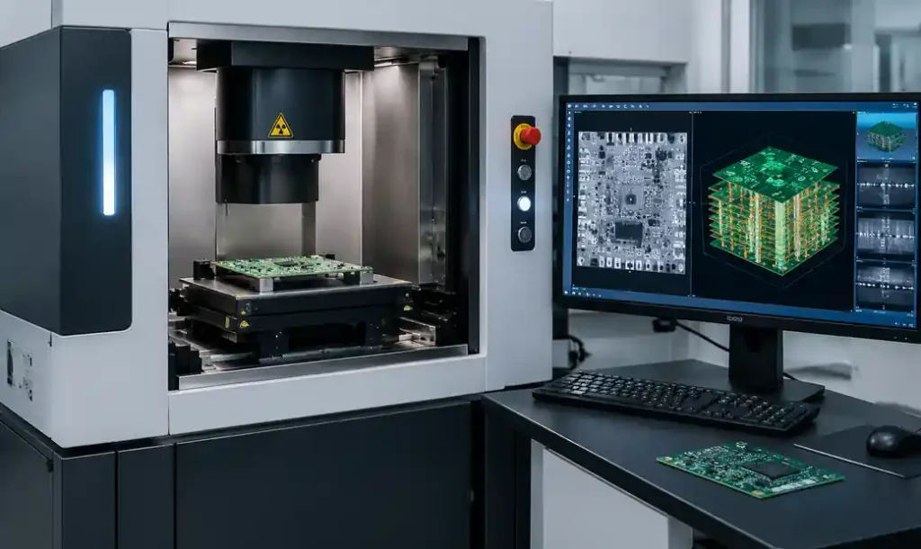
Modern X-ray systems achieve resolution down to 1 micron for analyzing high-density interconnect (HDI) designs with laser-drilled microvias. Automated 3D segmentation processes X-ray CT data to extract netlist information and component connectivity.
High-Resolution Imaging
Optical microscopy with 10x to 200x magnification captures copper trace patterns, pad geometries, and silkscreen markings. Image stitching software combines photographs into complete board maps for manual trace-out or automated netlist extraction.
Destructive Analysis Methods
Microsectioning
Cross-sectional analysis through microsectioning reveals internal layer structures, via plating quality, and material compositions. This technique provides critical information about layer count, copper weights (0.5oz to 6oz), dielectric thicknesses, and via aspect ratios.
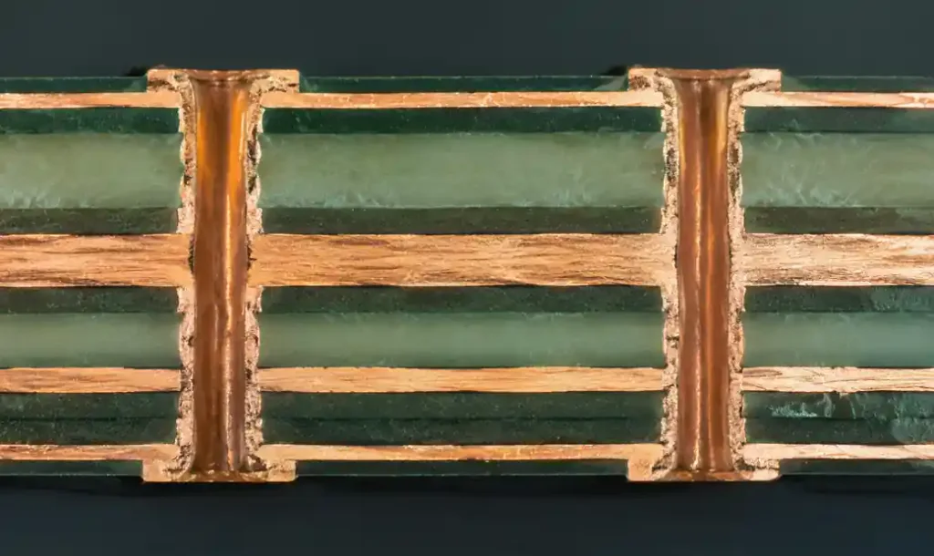
According to IPC-TM-650 standards, microsectioning validates manufacturing quality and investigates failure mechanisms. You will need this method when determining exact stackup configurations for PCB manufacturing or analyzing solder joint quality per IPC-A-610 criteria.
Layer Separation
Chemical etching removes individual copper layers sequentially for documentation of internal routing patterns. This method works best for 4-8 layer boards where X-ray resolution proves insufficient. While providing complete routing visibility, it destroys the original PCB.
Netlist Extraction and Schematic Recreation
Modern software tools process PCB images to identify component locations, trace connectivity, and generate netlist files. Automated extraction reduces manual trace-out time by 60-80% compared to traditional methods.
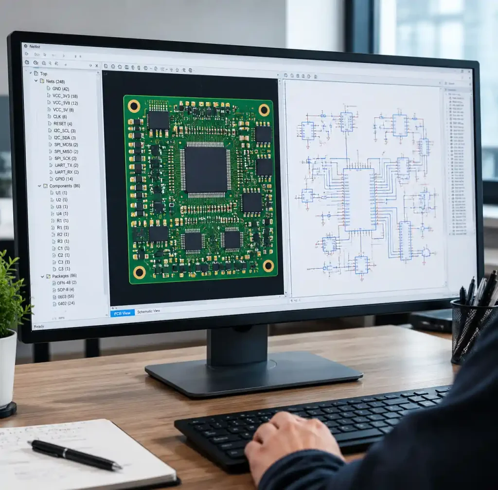
The workflow includes component identification through optical character recognition (OCR), copper trace vectorization, netlist generation mapping pins to traces, and schematic capture. Validation requires electrical testing to confirm netlist accuracy before using results for PCB design reproduction.
Component Identification and Bill of Materials
Part Number Recognition
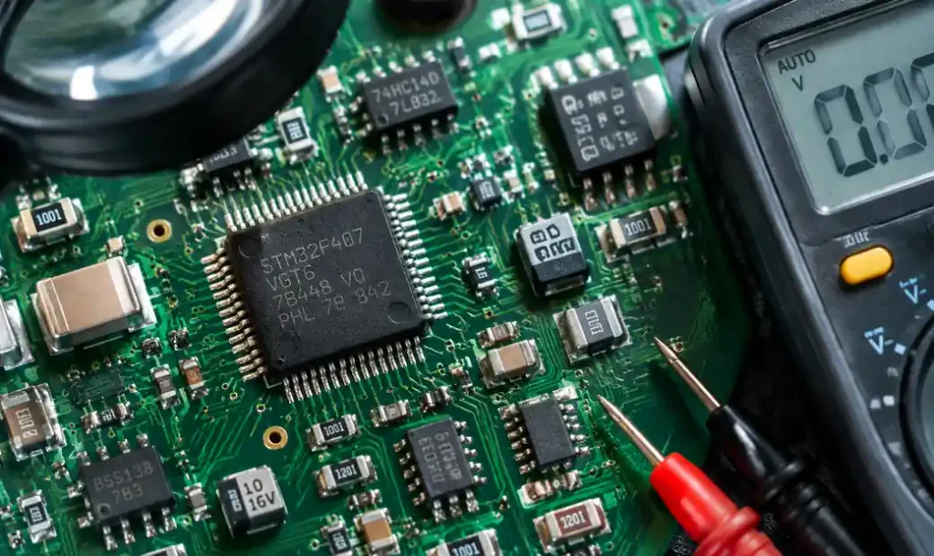
Surface-mount components carry identifying markings that vary by manufacturer and package type. Integrated circuits typically display full part numbers, while passive components use abbreviated codes requiring cross-reference databases for identification.
You can identify resistors and capacitors through physical measurement combined with marking code lookup. For unmarked components, electrical testing determines approximate values, though precise specifications may require component removal and bench testing.
Creating Accurate BOMs
A complete bill of materials (BOM) lists every component with manufacturer part numbers, quantities, reference designators, and specifications. This documentation enables sourcing replacement parts for repairs or fabricating compatible designs.
| Component Category | Identification Method | Typical Success Rate |
|---|---|---|
| ICs with Markings | Part number lookup | 95%+ |
| Passive Components | Measurement + marking codes | 80-90% |
| Connectors | Physical measurement + type identification | 85-95% |
| Unmarked Components | Electrical testing + circuit analysis | 50-70% |
| Obsolete Parts | Cross-reference to modern equivalents | 60-80% |
When original part numbers are obsolete, you must identify functionally equivalent replacements with matching electrical specifications, package footprints, and reliability ratings.
Applications and Use Cases
Obsolete Product Support
Legacy industrial equipment and medical devices often require maintenance long after manufacturers discontinue production. Original component suppliers may cease manufacturing specific parts, forcing equipment owners to reverse engineer boards for reproduction using available components. Many medical device manufacturers maintain legacy system support for 15-25 years through controlled reverse engineering programs.
Failure Analysis and Quality Investigation
When PCBs fail in the field, reverse engineering combined with PCB testing methods identifies root causes. Failure analysis for automotive, aerospace, and medical applications follows strict protocols per IPC-6012 Class 3 requirements.
Interoperability and Interface Development
Creating compatible accessories for existing systems requires understanding interface specifications that manufacturers do not publicly document. Reverse engineering the interface circuitry provides necessary electrical characteristics. This falls under fair use when developing products that work with but do not replicate the original system.
Frequently Asked Questions
Is PCB reverse engineering legal?
Yes, PCB reverse engineering is legal in most jurisdictions when performed on lawfully purchased products for legitimate purposes including obsolete product support, failure analysis, interoperability research, and educational study. However, using reverse-engineered designs to manufacture competing commercial products typically violates intellectual property rights.
What information can X-ray inspection reveal?
X-ray computed tomography reveals internal layer structures, buried via locations, inner layer routing patterns, and component placement on multilayer PCBs. Modern systems achieve 1-micron resolution sufficient for analyzing HDI boards with microvias. X-ray inspection is non-destructive and preserves board functionality after examination.
How accurate is automated netlist extraction?
Automated netlist extraction from PCB images typically achieves 85-95% accuracy for boards with clear trace visibility and standard component packages. Complex high-density designs with fine-pitch BGAs and multilayer routing may require manual verification. Electrical testing should validate extracted netlists before using results for circuit reproduction.
When is microsectioning necessary?
Microsectioning is necessary when you need exact stackup information including layer count, copper weights, dielectric thicknesses, and via construction details that surface inspection cannot determine. This destructive method is essential for failure analysis investigations and validating manufacturing processes per IPC-TM-650 test methods.
Can I reverse engineer patented PCB designs?
Reverse engineering to understand patented designs is legal, but manufacturing products based on patented circuit topologies without licensing constitutes patent infringement. You should conduct freedom-to-operate analysis and consult intellectual property counsel before commercializing designs derived from patented products.
What tools do I need for PCB reverse engineering?
Basic reverse engineering requires high-resolution camera equipment, optical microscope with 10-200x magnification, multimeter for continuity testing, and netlist extraction software. Advanced analysis may need X-ray CT scanning systems, microsectioning equipment, and automated image processing tools for complex multilayer boards.
Conclusion
PCB reverse engineering serves legitimate purposes in maintaining legacy systems, investigating failures, and developing compatible products when original documentation is unavailable. The process combines non-destructive methods like X-ray imaging with destructive techniques to extract complete design information.
Legal considerations require understanding fair use principles and patent rights. Reverse engineering lawfully purchased products for interoperability, repair, or security research generally receives legal protection, while commercial cloning violates intellectual property rights.
The technical process involves component identification, netlist extraction through automated tools, and schematic recreation validated through electrical testing. Modern X-ray CT systems enable efficient analysis of complex multilayer designs.
If you need high-quality PCB manufacturing for reverse-engineered designs or replacement boards for obsolete equipment, Andwin Circuits offers advanced manufacturing capabilities up to 50 layers with fast turnaround in 7 days. Our facility is certified to ISO 9001, IATF 16949, and UL standards for automotive, medical, telecommunications, and industrial applications worldwide.
Contact us today for custom PCB solutions, technical specifications, and competitive factory-direct pricing.