
PCB Solder Mask: Color Selection, LPI vs LPISM, and Design Guidelines
Solder mask failures account for 18% of PCB manufacturing defects, with misaligned openings causing assembly delays and rework costs. At Andwin Circuits, production data shows proper solder mask design delivers 97-99% first-pass yield versus 85-92% for marginal designs.
Choosing the right color, understanding LPI versus LPISM, and applying correct dam width and expansion rules determine whether your board solders reliably. This guide provides practical specifications based on IPC-SM-840 standards and manufacturing experience.
What Is Solder Mask and Why It Matters
Solder mask is a thin polymer layer applied over copper traces, leaving pads, vias, and test points exposed. It prevents solder bridges during reflow—exposed copper between fine-pitch pads would wick molten solder, creating shorts. Properly applied solder mask reduces bridge defects by over 95%.

It provides electrical insulation withstanding 500V or higher per IPC-SM-840 Class 3, protects copper from oxidation that degrades solderability, and improves mechanical durability by resisting abrasion during handling.
LPI Solder Mask: The Industry Standard
Liquid Photoimageable (LPI) solder mask dominates PCB manufacturing, delivering precise registration at competitive cost. The process applies liquid epoxy ink over copper through screen coating, creating 15-35 micron wet film.
UV exposure through a phototool cross-links the epoxy where light reaches, leaving unexposed areas uncured. Development spray washes away uncured mask, leaving openings over pads with ±75 micron (±3 mil) registration accuracy.

Thermal curing at 140-160°C for 60-90 minutes completes cross-linking, achieving final strength and IPC-SM-840 properties. LPI reliably processes 0.4mm pitch BGA patterns and 4 mil (0.1mm) solder mask dams—geometries impossible with older methods.
LPISM: Same Process, Different Name
LPISM (Liquid Photoimageable Solder Mask) is identical to LPI—both describe liquid polymer application, UV photoimaging, development, and thermal cure. The terminology is interchangeable.
Manufacturers sometimes use “LPISM” to distinguish from older dry film masks, but modern “LPI” already means liquid application. Treat them as identical and focus on the manufacturer’s process control—exposure calibration, developer monitoring, and cure verification.
Solder Mask Color Selection
Color selection affects inspection efficiency, thermal performance, and aesthetics. Eight colors dominate production, each with specific advantages.
Green: The Manufacturing Standard
Green represents over 70% of production volume due to mature processes and excellent inspection characteristics. The human eye exhibits maximum sensitivity to green wavelengths around 555nm, making defects easier to detect during optical inspection.
Green provides optimal contrast with white silkscreen and gold or silver finishes. Manufacturing cost is lowest because high volumes drive ink pricing down, and lead time is shortest since fabricators maintain continuous stock.
White: Maximum Light Reflection for LED Applications
White solder mask reflects 75-85% of incident light versus 8-12% for green and 2-5% for black. This makes white preferred for LED lighting where efficiency matters—the PCB surface acts as a secondary reflector, maximizing lumens per watt.
However, white requires careful thermal control during reflow—excessive heat causes yellowing. Specify 245°C peak temperature maximum versus 260°C for green. White also shows contamination readily, requiring enhanced cleaning to maintain cosmetic quality.
Matte Black: Premium Aesthetics for Consumer Electronics
Matte black delivers sophisticated appearance valued in premium consumer electronics—gaming hardware, audio equipment, and visible circuit boards. The non-reflective surface creates visual depth consumers associate with quality.
Black provides excellent contrast for white or metallic silkscreen, making logos striking. The matte finish reduces light reflection, valuable near optical sensors. Dark surfaces exhibit slightly higher thermal emissivity, though this doesn’t replace proper thermal management.

Manufacturing includes 10-15% price premium over green and longer lead times. Black requires careful exposure control to achieve complete cure.
Color Comparison Table
| Color | Light Reflection | Inspection Contrast | Cost vs Green | Best Applications |
|---|---|---|---|---|
| Green | 8-12% | Excellent | Baseline | General electronics, high reliability |
| White | 75-85% | Good | +15-25% | LED lighting, high-brightness displays |
| Matte Black | 2-5% | Excellent | +10-15% | Consumer electronics, premium products |
| Red | 15-20% | Good | +15-20% | Power supplies, automotive, branding |
| Blue | 10-15% | Good | +15-20% | Aerospace, marine, product differentiation |
Solder Mask Dam Width: Design Rules
Solder mask dam width refers to the polymer strip between adjacent pad openings. This bridge must withstand assembly stress, thermal cycling, and operation without cracking.
Standard LPI processes reliably produce 4 mil (0.1mm) dams. Tighter 3 mil (0.075mm) dams are achievable with advanced equipment but reduce yield and increase cost. Dense layouts with fine-pitch components present challenges—a 0.5mm pitch BGA with 0.3mm pads and 3 mil expansion leaves only 0.05mm (2 mil) dam width, below reliable limits.

Calculate dam width:
Dam Width = Pad Pitch – Pad Diameter – (2 × Solder Mask Expansion)
Example: 0.65mm pitch QFN with 0.35mm pads and 3 mil (0.076mm) expansion:
- Dam Width = 0.65 – 0.35 – (2 × 0.076) = 0.148mm (5.8 mil) ✓
Example: 0.5mm pitch with same pads:
- Dam Width = 0.5 – 0.35 – (2 × 0.076) = 0.048mm (1.9 mil) ✗
| Component Pitch | Typical Pad Size | Max Expansion | Resulting Dam Width |
|---|---|---|---|
| ≥0.8mm | 0.4mm | 4 mil (0.1mm) | ≥6 mil (0.15mm) |
| 0.65mm | 0.35mm | 3 mil (0.076mm) | ≥5 mil (0.13mm) |
| 0.5mm | 0.3mm | 2 mil (0.05mm) | ≥4 mil (0.1mm) |
| 0.4mm | 0.25mm | 2 mil (0.05mm) | ≥3 mil (0.075mm) |
For ultra-fine pitch below 0.4mm, consider solder mask defined (SMD) pads where the mask opening is smaller than the copper pad, controlling solder paste through the mask rather than stencil.
Solder Mask Expansion: Balancing Exposure and Alignment
Solder mask expansion defines the intentional gap between copper pad edges and mask opening edges. Positive expansion (mask opening larger than pad) is standard, ensuring full pad exposure while accommodating misalignment.
Standard expansion is 3-4 mil (0.076-0.1mm) for surface mount pads, providing tolerance for typical ±3 mil registration accuracy.
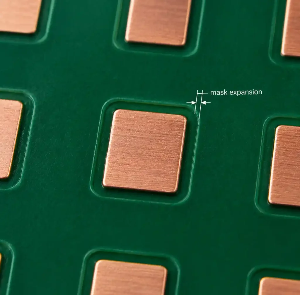
Too large expansion exposes copper traces near pads, increasing oxidation risk and creating unintended solder wicking. Gaps wider than 6 mil may allow bridges on fine-pitch components.
Too small expansion creates weak solder joints. If the mask barely clears the pad or overlaps, joints form on partially masked copper with degraded wetting, producing failures during thermal cycling.
High-density designs require reduced expansion. For components below 0.5mm pitch (BGA, QFN, CSP), specify 2-2.5 mil (0.05-0.063mm) expansion. This prevents bridging while maintaining adequate copper exposure.
Tented vias (mask completely covers holes) use negative expansion. Untented vias expose holes for plugging or test access, requiring standard positive expansion.
IPC-SM-840 Standards
IPC-SM-840E establishes material requirements and testing for solder mask. Three classes match IPC-6012:
Class 1: Basic adhesion, thermal resistance to 105°C. For consumer electronics.
Class 2: Thermal shock to 288°C (six cycles), enhanced moisture and insulation resistance. For commercial and industrial equipment—most applications.
Class 3: Ten thermal shock cycles, superior insulation. For aerospace, military, and medical devices.
Key tests include cross-hatch adhesion, thermal shock cycling, UL 94 V-0 flammability, and insulation resistance >10^9 ohms for Class 3. Specify Class 2 for most applications, Class 3 for high reliability.
Design Guidelines

Maintain Minimum Clearances: Keep mask-to-trace spacing at 2 mil (0.05mm) minimum to prevent unintentional coverage and adhesion failures.
Avoid Thin Dams: Design for 4 mil (0.1mm) minimum dam width. Consult your fabricator for 3 mil dams, which need enhanced controls and increase cost.
Define Via Treatment: Specify tented (covered), untented (exposed), or plugged vias. Tented reduces steps but may trap flux. Untented allows via-in-pad. Plugged prevents wicking but adds cost.
Match Expansion to Pitch: Use 3-4 mil for standard components (≥0.65mm pitch), 2-2.5 mil for fine-pitch (<0.5mm pitch).
Verify Color Requirements: For white, limit reflow to 245°C maximum and request enhanced cleaning. For black, confirm exposure and cure parameters.
Manufacturing at Andwin Circuits
Andwin Circuits manufactures PCBs with LPI solder mask in multiple colors at our IATF 16949 certified facility. Our automated coating lines apply 25-micron ±5-micron thickness with ±75-micron registration, reliably producing 4 mil dams and supporting 0.4mm pitch patterns.
We stock Rogers and aluminum substrates for Metal Core PCB and LED PCB applications. Our engineering team provides DFM reviews verifying solder mask clearances and dam widths. Quick-turn prototypes ship in 24-72 hours.
FAQ
What is the difference between LPI and LPISM solder mask?
LPI and LPISM are identical—both describe liquid photoimageable solder mask applied as liquid epoxy, UV exposed, chemically developed, and thermally cured. Focus on the manufacturer’s registration accuracy and minimum dam capability rather than naming conventions.
Which solder mask color is best for LED PCBs?
White solder mask reflects 75-85% of incident light versus 8-12% for green, making it optimal for LED lighting. The white surface acts as a secondary reflector, improving lumens per watt. Specify 245°C maximum reflow temperature to prevent yellowing.
What is the minimum solder mask dam width for fine-pitch BGAs?
Standard LPI processes reliably produce 4 mil (0.1mm) dams. Fine-pitch BGAs below 0.5mm pitch often require 3 mil (0.075mm) dams with advanced controls. For 0.4mm pitch and below, consider solder mask defined pads. Always verify with your fabricator’s capability.
How much solder mask expansion should I use for standard SMT components?
Use 3-4 mil (0.076-0.1mm) expansion for components with 0.65mm pitch or greater. This accommodates typical ±3 mil registration tolerance. For fine-pitch devices below 0.5mm pitch, reduce to 2-2.5 mil to maintain adequate dam width.
Does solder mask color affect thermal performance?
Solder mask color has minimal impact—copper thickness and thermal vias provide greater benefit. Darker colors exhibit slightly higher thermal emissivity, while white reflects more light in LED applications. For boards dissipating over 5W, focus on PCB thermal management techniques.
What IPC-SM-840 class should I specify?
Specify Class 2 for commercial and industrial electronics—this covers most applications. Class 3 applies to aerospace, military, and medical devices. Class 1 suffices only for short-life consumer electronics. When in doubt, specify Class 2.
Conclusion
Solder mask selection and design directly determine PCB yield and reliability. Green remains the standard for inspection contrast and cost, while white optimizes LED applications through light reflection. Matte black delivers premium aesthetics for consumer electronics.
LPI solder mask dominates production because photoimaging delivers precise registration for fine-pitch designs. Maintain 4 mil minimum dam width, apply 3-4 mil expansion for standard pitch (2-2.5 mil for fine pitch), and specify IPC-SM-840 Class 2 or Class 3. Verify color-specific requirements with your fabricator.
Andwin Circuits manufactures PCBs with controlled solder mask processing in multiple colors with 24-72 hour quick-turn prototypes. Contact us for your PCB manufacturing needs with competitive factory-direct pricing.